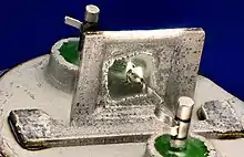
Alloy-junction transistor
The germanium alloy-junction transistor, or alloy transistor, was an early type of bipolar junction transistor, developed at General Electric and RCA in 1951 as an improvement over the earlier grown-junction transistor.


The usual construction of an alloy-junction transistor is a germanium crystal forming the base, with emitter and collector alloy beads fused on opposite sides. Indium and antimony were commonly used to form the alloy junctions on a bar of N-type germanium. The collector junction pellet would be about 50 mils (thousandths of an inch) in diameter, and the emitter pellet about 20 mils. The base region would be on the order of 1 mil (0.001 inches, 25 μm) thick.[1] There were several types of improved alloy-junction transistors developed over the years that they were manufactured.
All types of alloy-junction transistors became obsolete in the early 1960s, with the introduction of the planar transistor which could be mass-produced easily while alloy-junction transistors had to be made individually. The first germanium planar transistors had much worse characteristics than alloy-junction germanium transistors of the period, but they cost much less, and the characteristics of planar transistors improved very rapidly, quickly exceeding those of all earlier germanium transistors.
Micro-alloy transistor
The micro-alloy transistor (MAT) was developed by Philco as an improved type of alloy-junction transistor, it offered much higher speed.
It is constructed of a semiconductor crystal forming the base, into which a pair of wells are etched (similar to Philco's earlier surface-barrier transistor) on opposite sides then fusing emitter and collector alloy beads into the wells.
Micro-alloy diffused transistor
The micro-alloy diffused transistor (MADT), or micro-alloy diffused-base transistor, was developed by Philco as an improved type of micro-alloy transistor; it offered even higher speed. It is a type of diffused-base transistor.
Before using electrochemical techniques and etching depression wells into the base semiconductor crystal material, a heated diffused phosphorus gaseous layer is created over the entire intrinsic semiconductor base crystal, creating a N-type graded base semiconductor material. The emitter well is etched very shallow into this diffused base layer.
For high-speed operation, the collector well is etched all the way through the diffused base layer and through most of the intrinsic base semiconductor region, forming an extremely thin base region.[2][3] A doping-engineered electric field was created in the diffused base layer to reduce the charge carrier base transit time (similar to the drift-field transistor).
Post-alloy diffused transistor
The post-alloy diffused transistor (PADT), or post-alloy diffused-base transistor, was developed by Philips (but GE and RCA filed for patent and Jacques Pankove of RCA received patent for it) as an improvement to the germanium alloy-junction transistor, it offered even higher speed. It is a type of diffused-base transistor.
The Philco micro-alloy diffused transistor had a mechanical weakness that ultimately limited their speed; the thin diffused base layer would break if made too thin, but to get high speed it needed to be as thin as possible. Also it was very hard to control alloying on both sides of such a thin layer.
The post-alloy diffused transistor solved this problem by making the bulk semiconductor crystal the collector (instead of the base), which could be as thick as necessary for mechanical strength. The diffused base layer was created on top of this. Then two alloy beads, one P-type and one N-type were fused on top of the diffused base layer. The bead having the same type as the base dopant then became part of the base and the bead having the opposite type from the base dopant became the emitter.
A doping-engineered electric field was created in the diffused base layer to reduce the charge carrier base transit time (similar to the drift-field transistor).
Photo gallery
 TG 51 PNP germanium alloy transistor Made by TEWA Poland
 TG 51 PNP germanium alloy transistor Made by TEWA Poland
 General Electric 2N1307 PNP germanium alloy transistor
 General Electric 2N1307 PNP germanium alloy transistor
 RCA 2N404 Germanium PNP Transistor. Medium Speed Switch
 PNP germanium alloy transistor intended as AF amplifier / switch
See also
References
- Lloyd P. Hunter (ed.), Handbook of Semiconductor Electronics, Mc Graw Hill, 1956 pp. 7–18, 7–19
- A High Frequency Transistor Analysis by James K. Keihner, 1956
- Wall Street Journal, Article: "Philco Says It Is Producing A New Kind Of Transistor", October 9, 1957, pg 19