Alpha 21064
The Alpha 21064 is a microprocessor developed and fabricated by Digital Equipment Corporation that implemented the Alpha (introduced as the Alpha AXP) instruction set architecture (ISA). It was introduced as the DECchip 21064 before it was renamed in 1994. The 21064 is also known by its code name, EV4. It was announced in February 1992 with volume availability in September 1992. The 21064 was the first commercial implementation of the Alpha ISA, and the first microprocessor from Digital to be available commercially. It was succeeded by a derivative, the Alpha 21064A in October 1993. This last version was replaced by the Alpha 21164 in 1995.
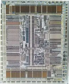
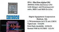
History
The first Alpha processor was a test chip codenamed EV3. This test chip was fabricated using Digital's 1.0-micrometre (μm) CMOS-3 process. The test chip lacked a floating point unit and only had 1 KB caches. The test chip was used to confirm the operation of the aggressive circuit design techniques. The test chip, along with simulators and emulators, was also used to bring up firmware and the various operating systems that the company supported.
The production chip, codenamed EV4, was fabricated using Digital's 0.75 μm CMOS-4 process. Dirk Meyer and Edward McLellan were the micro-architects. Ed designed the issue logic while Dirk designed the other major blocks. Jim Montanaro led the circuit implementation. The EV3 was used in the Alpha Demonstration Unit (ADU), a multiprocessor system used by Digital to develop software for the Alpha platform before the availability of EV4 parts.[1]
The 21064 was unveiled at the 39th International Solid-State Circuits Conference (ISSCC) in mid-February 1992. It was announced on 25 February 1992, with a 150 MHz sample introduced on the same day. It was priced at $3,375 in quantities of 100, $1,650 in quantities between 100 and 1,000, and $1,560 for quantities over 1,000. Volume shipments began in September 1992.
In early February 1993, the price of the 150 MHz version was reduced to $1,096 from $1,559 in quantities greater than 1,000.
On 25 February 1993, a 200 MHz was introduced, with sample kits available, priced at $3,495. In volume, it was priced at $1,231 per unit in quantities greater than 10,000. Volume orders were accepted in June 1993, with shipments in August 1993. The price of the 150 MHz version was reduced in response. The sample kit was reduced to $1,690 from $3,375, effective in April 1993; and in volume, it was reduced to $853 from $1,355 per unit in quantities greater than 10,000, effective in July 1993.
With the introduction of the Alpha 21066 and the Alpha 21068 on 10 September 1993, Digital adjusted the positioning of the existing 21064s and introduced a 166 MHz version priced at $499 per unit in quantities of 5,000. The price of the 150 MHz version was reduced to $455 per unit in quantities of 5,000.
On 6 June 1994, the price of the 200 MHz version was reduced by 31% to $544 to position it against the 60 MHz Pentium; and the 166 MHz version by 19% to $404 per unit in quantities of 5,000, effective on 3 July 1994.
The Alpha 21064 was fabricated at Digital's Hudson, Massachusetts and South Queensferry, Scotland facilities.
Users
The 21064 was mostly used in high-end computers such as workstations and servers. Users included:
- Aspen Systems in its Alpine workstations
- Carrera Computers in its Hercules 150, Hercules 200, and Pantera II workstations
- Cray Research, which used the 150 MHz 21064 in its Cray T3D supercomputers
- Digital, in its DECpc AXP 150 entry-level workstations, DEC 2000 AXP entry-level servers, DEC 3000 AXP workstations and entry-level servers, DEC 4000 AXP mid-range servers and DEC 7000/10000 AXP high-end servers
- Encore Computer, in its Infinity R/T high-end real-time computer
Performance
The 21064 was the highest performing microprocessor from when it was introduced until 1993, after International Business Machines (IBM) introduced the multi-chip POWER2. It subsequently became the highest performing single-chip microprocessor, a position it held until the 275 MHz 21064A was introduced in October 1993.[2]
Description
The Alpha 21064 is a superpipelined dual-issue superscalar microprocessor that executes instructions in-order. It is capable of issuing up to two instructions every clock cycle to four functional units: an integer unit, a floating-point unit (FPU), an address unit, and a branch unit. The integer pipeline is seven stages long, and the floating-point pipeline ten stages. The first four stages of both pipelines are identical and are implemented by the I-Box.
I-box
The I-box is the control unit; it fetches, decodes, and issues instructions and controls the pipeline.[3] During stage one, two instructions are fetched from the I-cache. Branch prediction is performed by logic in the I-box during stage two. Either static prediction or dynamic prediction is used. Static prediction examined the sign bit of the displacement field of a branch instruction, predicted the branch as taken if the sign bit indicated a backwards branch (if sign bit contained 1). Dynamic prediction examined an entry in the 2,048-entry by 1-bit branch history table. If an entry contained 1, the branch was predicted as taken.[4] If dynamic prediction was utilized, the branch prediction is approximately 80% accurate for most programs.[5] The branch misprediction penalty is four cycles.[6]
These instructions are decoded during stage three. The I-box then checks if the resources required by the two instructions are available during stage four. If so, the instructions are issued, providing they can be paired. Which instructions could be paired was determined by the number of read and write ports in the integer register file.[7] The 21064 could issue: an integer operate with a floating-point operate, any load/store instruction with any operate instruction, an integer operate with an integer branch, or a floating-point operate with a floating-point branch. Two combinations were not permitted: an integer operate and a floating-point store, and a floating-point operate and an integer store. If one of the two instructions cannot be issued together, the first four stages are stalled until the remaining instruction is issued. The first four stages are also stalled in the event that no instruction can be issued due to resource unavailability, dependencies, or similar conditions.
The I-box contains two translation lookaside buffers (TLBs) for translating virtual addresses to physical addresses. These TLBs are referred to as instruction translation buffers (ITBs). The ITBs cache recently used page table entries for the instruction stream. An eight-entry ITB is used for 8 KB pages and a four-entry ITB for 4 MB pages. Both ITBs are fully associative and use a not-last used replacement algorithm.[8]
Execution
Execution begins during stage five for all instructions. The register files are read during stage four. The pipelines beginning at stage five cannot be stalled.
Integer unit
The integer unit is responsible for executing integer instructions. It consists of the integer register file (IRF) and the E-box. The IRF contains thirty-two 64-bit registers and has four read ports and two write ports that are equally divided between the integer unit and the branch unit.[9] The E-box contains an adder, a logic unit, barrel shifter, and multiplier. Except for multiply, shift, and byte manipulation instructions, most integer instructions are completed by the end of stage five and thus have a latency of one cycle. The barrel shifter is pipelined, but shift and byte manipulation instructions are not completed by the end of stage six, and thus have a latency of two cycles. The multiplier was not pipelined in order to save die area;[5] thus multiply instructions have a variable latency of 19 to 23 cycles depending on the operands. In stage seven, integer instructions write their results to the IRF.
Address unit
The address unit, also known as the "A-box", executed load and store instructions. To enable the address unit and integer unit to operate in parallel, the address unit has its own displacement adder, which it uses to calculate virtual addresses, instead of using the adder in the integer unit.[10] A 32-entry fully associative translation lookaside buffer (TLB) is used to translate virtual addresses into physical addresses.[10] This TLB is referred to as the data translation buffer (DTB). The 21064 implemented a 43-bit virtual address and a 34-bit physical address, and is therefore capable of addressing 8 TB of virtual memory and 16 GB of physical memory.
Store instructions result in data buffered in a 4-entry by 32-byte write buffer. The write buffer improved performance by reducing the number of writes on the system bus by merging data from adjacent stores and by temporarily delaying stores, enabling loads to be serviced quicker as the system bus is not utilized as often.[10]
Floating-point unit
The floating-point unit consists of the floating-point register file (FRF) and the F-box.[7] The FRF contains thirty-two 64-bit registers and has three read ports and two write ports. The F-box contained a floating-point pipeline and a non-pipelined divide unit which retired one bit per cycle.
The floating-point register file is read and the data formatted into fraction, exponent, and sign in stage four. If executing add instructions, the adder calculates the exponent difference, and a predictive leading one or zero detector using input operands for normalizing the result is initiated. If executing multiply instructions, a 3 X multiplicand is generated.
In stages five and six, alignment or a normalization shift and sticky-bit calculations are performed for adds and subtracts. Multiply instructions are multiplied in a pipelined, two-way interleaved array which uses a radix-8 Booth algorithm.[5][11] In stage eight, final addition is performed in parallel with rounding. Floating-point instructions write their results to the FRF in stage ten.[11]
Instructions executed in the pipeline have a six-cycle latency.[11] Single-precision (32-bit) and double-precision (64-bit) divides, which are executed in the non-pipelined divide unit, have a latency of 31 and 61 cycles, respectively.[12]
Caches
The 21064 has two on-die primary caches: an 8 KB data cache (known as the D-cache) using a write-through write policy and an 8 KB instruction cache (known as the I-cache). Both caches are direct-mapped for single-cycle access and have 32-byte line size. The caches are built with six-transistor static random access memory (SRAM) cells that have an area of 98 μm2. The caches are 1,024 cells wide by 66 cells tall, with the top two rows used for redundancy.
An optional external secondary cache, known as the B-cache, with capacities of 128 KB to 16 MB was supported. The cache operated at one-third to one-sixteenth of the internal clock frequency, or 12.5 to 66.67 MHz at 200 MHz.[13] The B-cache is direct-mapped and has a 128-byte line size by default that could be configured to use larger quantities. The B-cache is accessed via the system bus.
External interface
The external interface is a 128-bit data bus that operated at half to one-eighth the internal clock rate, or 25 to 100 MHz at 200 MHz. The width of the bus was configurable, systems using the 21064 could have a 64-bit external interface. The external interface also consisted of a 34-bit address bus.
Fabrication
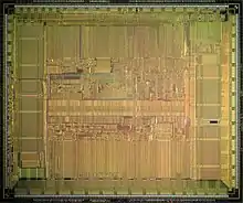
The 21064 contained 1.68 million transistors.[14] The original EV4 was fabricated by Digital in its CMOS-4 process, which has a 0.75 μm feature size and three levels of aluminium interconnect.[14] The EV4 measures 13.9 mm by 16.8 mm, for an area of 233.52 mm2. The later EV4S was fabricated in CMOS-4S, a 10% optical shrink of CMOS-4 with a 0.675 μm feature size. This version measured 12.4 mm by 15.0 mm, for an area 186 mm2.[15]
The 21064 used a 3.3-volt (V) power supply.[14] The EV4 dissipated a maximum of 30 W at 200 MHz. The EV4S dissipates a maximum of 21.0 W at 150 MHz, 22.5 W at 166 MHz, and 27.0 W at 200 MHz.[16]
Package
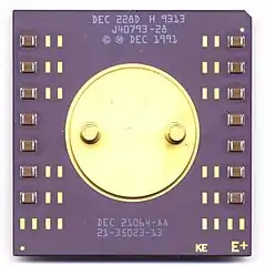
The 21064 is packaged in a 431-pin alumina-ceramic pin grid array (PGA) measuring 61.72 mm by 61.72 mm.[17] Of the 431 pins, 291 were for signals and 140 were for power and ground.[14][18] The heatsink is directly attached to the package, secured by nuts attached to two studs protruding from the tungsten heat spreader.
Derivatives
Alpha 21064A
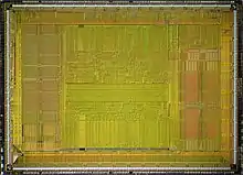
The Alpha 21064A, introduced as the DECchip 21064A, code-named EV45, is a further development of the Alpha 21064 introduced in October 1993. It operated at clock frequencies of 200, 225, 233, 275 and 300 MHz. The 225 MHz model was replaced by the 233 MHz model on 6 July 1994, which at introduction, was priced at US$788 in quantities of 5,000, 10% less than the 225 MHz model it replaced. On the same day, prices for the 275 MHz was also reduced by 25% to US$1,083 in quantities of 5,000. The 300 MHz model was announced and sampled on 2 October 1995 and was shipped in December 1995. There was also one model, the 21064A-275-PC, that was restricted to running the Windows NT or operating systems that use the Windows NT memory management model.
The 21064A succeeded the original 21064 as the high-end Alpha microprocessor. It subsequently saw the most use in high-end systems. Users included:
- Digital in some models of its DEC 3000 AXP, DEC 4000 AXP and DEC 7000/10000 AXP systems
- Aspen Systems in its Alpine workstation
- BTG, who used a 275 MHz model in its Action AXP275 RISC PC
- Carrera Computers in its Cobra AXP 275 workstation
- NekoTech, who used a 275 MHz model overclocked by 5% to 289 MHz in their Mach 2-289-T workstation
- Network Appliance (now NetApp), who used a 275 MHz model in its storage systems
The 21064A had a number of microarchitectural improvements over the 21064. The primary caches were improved in two ways: the capacity of the I-cache and D-cache was doubled from 8 KB to 16 KB and parity protection was added to the cache tag and cache data arrays. Floating-point divides have a lower latency due to an improved divider that retires two bits per cycle on average. Branch prediction was improved by a larger 4,096-entry by 2-bit BHT.
The 21064A contains 2.8 million transistors and is 14.5 by 10.5 mm large, for an area of 152.25 mm2. It was fabricated by Digital in their fifth-generation CMOS process, CMOS-5, a 0.5 μm process with four levels of aluminium interconnect.[19]
Alpha 21066
The Alpha 21066, introduced as the DECchip 21066, code-named LCA4 (Low Cost Alpha), is a low-cost variant of Alpha 21064. Samples were introduced on 10 September 1993, with volume shipments in early 1994. At the time of introduction, the 166 MHz Alpha 21066 was priced at US$385 in quantities of 5,000. A 100 MHz model, intended for embedded systems, also existed. Sampling begun in late 1994, with volume shipments in the third quarter of 1995. The Microprocessor Report recognized the Alpha 21066 as the first microprocessor with an integrated PCI controller.
The Alpha 21066 was intended for use in low-cost applications, specifically personal computers running Windows NT. Digital used various models of the Alpha 21066 in their Multia clients, AXPpci 33 original equipment manufacturer (OEM) motherboards and AXPvme single-board computers. Outside of Digital, users included Aspen Systems in its Alpine workstation, Carrera Computers in its Pantera I workstation, NekoTech used a 166 MHz model in its Mach 1-166 personal computer, and Parsys in its TransAlpha TA9000 Series supercomputers.
Due to the process shrink, it was able to include features that were desirable in cost-sensitive embedded systems. These features include an on-die B-cache and memory controller with ECC support, a functionally limited graphics accelerator supporting up to 8 MB of VRAM for implementing a framebuffer, a PCI controller and a phase-locked loop (PLL) clock generator for multiplying a 33 MHz external clock signal to the desired internal clock frequency.
The memory controller supported 64 KB to 2 MB of B-cache and 2 to 512 MB of memory. The ECC implementation was capable of detecting 1-, 2- and 4-bit errors and correcting 1-bit errors. To reduce cost, the Alpha 21066 has a 64-bit system bus, which reduced the number of pins and thus the size of the package. The reduced width of the system bus also reduced bandwidth and thus performance by 20%, which was deemed acceptable.
The 21066 contained 1.75 million transistors and measured 17.0 by 12.3 mm, for an area of 209.1 mm2. It was fabricated in CMOS-4S, a 0.675 μm process with three levels of interconnect. The 21066 was packaged in a 287-pin CPGA measuring 57.404 by 57.404 mm.
Alpha 21066A

The Alpha 21066A, code-named LCA45, is a low-cost variant of the Alpha 21064A. It was announced on 14 November 1994, with samples of 100 and 233 MHz models introduced on the same day. Both models were shipped in March 1995. When announced, the 100 and 233 MHz models were priced at $175 and $360, respectively, in quantities of 5,000. A 266 MHz model was later made available.
The 21066A was second sourced by Mitsubishi Electric as the M36066A. It was the first Alpha microprocessor to be fabricated by the company. 100 and 233 MHz parts were announced in November 1994. At the time of the announcement, engineering samples were set for December 1994, commercial samples in July 1995 and volume quantities in September 1995. The 233 MHz part was priced at $490 in quantities of 1,000.[20]
Although it was based on the 21064A, the 21066A did not have the 16 KB instruction and data caches. A feature specific to the 21066A was power management – the microprocessor's internal clock frequency could be adjusted by software.
Digital used various models of 21066A in their products which had previously used the 21066. Outside of Digital, Tadpole Technology used a 233 MHz model in their ALPHAbook 1 notebook.
The 21066A contained 1.8 million transistors on a die measuring 14.8 by 10.9 mm, for an area of 161.32 mm2. It was fabricated in Digital's fifth-generation CMOS process, CMOS-5, a 0.5 μm process with three levels of interconnect. Mitsubishi Electric fabricated the M36066A in its own 0.5 μm three-level-metal process.
Alpha 21068
The Alpha 21068, introduced as the DECchip 21068, is a version of the 21066 positioned for embedded systems. It was identical to the 21066 but had a lower clock rate to reduce power dissipation and cost. Samples were introduced on 10 September 1993 with volume shipments in early 1994. It operated at 66 MHz and had a 9 W maximum power dissipation. At the time of introduction, the 21068 was priced at US$221 each in quantities of 5,000. On 6 June 1994, Digital announced that it was cutting the price by 16% to US$186, effective on 3 July 1994.
The Alpha 21068 was used by Digital in their AXPpci 33 motherboard and the AXPvme 64 and 64LC single-board computers.
Alpha 21068A
The Alpha 21068A, introduced as the DECchip 21068A, is a variant of the Alpha 21066A for embedded systems. It operated at a clock frequency of 100 MHz.
Chipsets
Initially, there was no standard chipset for the 21064 and 21064A. Digital's computers used custom application-specific integrated circuits (ASICs) to interface the microprocessor to the system. As this raised development cost for third parties who wished to develop Alpha-based products, Digital developed a standard chipset, the DECchip 21070 (Apecs), for original equipment manufacturers (OEMs).
There were two models of the 21070, the DECchip 21071 and the DECchip 21072. The 21071 was intended for workstations whereas the 21072 was intended for high-end workstations or low-end uniprocessor servers. The two models differed in memory subsystem features: the 21071 has a 64-bit memory bus and supports 8 MB to 2 GB of parity-protected memory whereas the 21072 has a 128-bit memory bus and supports 16 MB to 4 GB of ECC-protected memory.
The chipset consisted of three chip designs: the COMANCHE B-cache and memory controller, the DECADE data slice, and the EPIC PCI controller. The DECADE chips implemented the data paths in 32-bit slices, and therefore the 21071 has two such chips while the 21072 has four. The EPIC chip has a 32-bit path to the DECADE chips.
The 21070 was introduced on 10 January 1994,[21] with samples available. Volume shipments began in mid-1994. In quantities of 5,000, the 21071 was priced at $90 and the 21072 at $120.
21070 users included Carrera Computers for its Pantera workstations and Digital in some models of its AlphaStations and uniprocessor AlphaServers.
See also
- AlphaVM: A full DEC Alpha system emulator running on Windows or Linux. It contains a high-performance emulator of the Alpha CPU.
Notes
- Charles P. Thacker; David G. Conroy; Lawrence C. Stewart (1992). "The Alpha Demonstration Unit: A High-performance Multiprocessor for Software and Chip Development" (PDF). Digital Technical Journal. 4 (4).
- Ryan 1994
- Digital Equipment Corporation 1996, p. 2-3–2-4
- Digital Equipment Corporation 1996, p. 2-5
- McLellan 1993, p. 42
- Dobberpuhl 1992, p. 37
- Dobberpuhl 1992, p. 36
- Digital Equipment Corporation 1996, p. 2-6
- Dobberpuhl 1992, pp. 35–36
- McLellan 1993, p. 43
- Dobberpuhl 1992, p. 38
- Gwennap 1994
- McLellan 1993, p. 44
- Dobberpuhl 1992, p. 35
- Bhandarkar 1995, pp. 2–4
- Digital Equipment Corporation 1996, p. 8-3
- Digital Equipment Corporation 1996, p. 8-2
- Bhandarkar 1995, p. 2
- Bhandarkar 1995, p. 3
- Krause 1994
- Digital Equipment Corporation 1994
References
- Alpha 21064 and 21064A Microprocessors Hardware Reference Manual, June 1996. Order number: EC-Q92UC-TE. Digital Equipment Corporation.
- Apiki, Steve; Grehan, Rick (March 1995). "Fastest NT Workstations". Byte.
- Bhandarkar, Dileep. "Alpha Implementations" Archived 24 May 2011 at the Wayback Machine, IEEE Computer Society Technical Committee on Computer Architecture Newsletter, December 1995.
- Computergram (25 February 1992). "DEC Reveals More On Alpha, Challenges Hewlett-Packard's Precision Architecture RISC". Computer Business Review.
- Computergram (26 February 1992). "DEC Describes Its Alpha RISC, Kubota Discloses Its Plans". Computer Business Review.
- Computergram (7 June 1994). "DEC slashes Alpha AXP Chip Prices by up to 31%". Computer Business Review.
- Computergram (13 September 1993). "DEC adds Alphas for Personal Computers, Control". Computer Business Review.
- Computergram (11 January 1994). "Microprocessor Report's Annual Chip Awards Declare Motorola 88110 the Part least likely to...". Computer Business Review.
- Computergram (11 November 1994). "Mitsubishi Electric Is Ready To Sample Its First Alpha At Last". Computer Business Review.
- Computergram (25 November 1994). "Mitsubishi's First Alpha Provides The Same Functionality As DEC's 21066A". Computer Business Review.
- Digital Equipment Corporation (10 January 1994). "Digital Introduces PCI-Based System Logic Chipsets For Alpha AXP 21064 Microprocessors And Announces The Industry's First PCI To PCI Bridge Chip". Press release.
- Dobberpuhl, Daniel W., Witek, Richard T. et al. "A 200-MHz 64-bit Dual-issue CMOS Microprocessor", Digital Technical Journal, Volume 4, Number 4, Special Issue 1992, pp. 35–50.
- Gwennap, Linley (12 September 1994). "Digital Leads the Pack with 21164", Microprocessor Report, Volume 8, Number 12.
- Krause, Reinhardt (13 September 1993). "DEC unveils two Alphas in PCI, embedded drive". Electronic News.
- Krause, Reinhardt (18 October 1993). "DEC readies 225/275MHz Alphas". Electronic News.
- Krause, Reinhardt (21 November 1994). "Alpha partners roll 233MHz 21066A". Electronic News.
- McKinney, Dina L. et al. "Digital's DECchip 21066: The First Cost-focused Alpha AXP Chip". Digital Technical Journal, Volume 6, Number 1, Winter 1994, pp. 66–77.
- McLellan, Edward (June 1993). "The Alpha AXP Architecture and 21064 Processor". IEEE Micro. pp. 36–47.
- Ryan, Bob; Thompson, Tom (January 1994). "RISC Grows Up". Byte.
Further reading
- "DEC Enters Microprocessor Business with Alpha". (4 March 1992). Microprocessor Report, Volume 6, Number 3.
- "DEC's Alpha Architecture Premiers". (4 March 1992). Microprocessor Report, Volume 6, Number 3.
- "Digital Plans Broad Alpha Processor Family" (18 November 1992). Microprocessor Report, Volume 6, Number 3.
- "Digital Reveals PCI Chip Sets For Alpha". (12 July 1993). Microprocessor Report, Volume 7, Number 9.
- "Alpha Hits Low End with Digital's 21066". (13 September 1993). Microprocessor Report, Volume 7, Number 12.
- Bhandarkar, Dileep P. (1995). Alpha Architecture and Implementations. Digital Press.
- Fox, Thomas F. (1994). "The design of high-performance microprocessors at Digital". Proceedings of the 31st Annual ACM-IEEE Design Automation Conference. pp. 586–591.
- Gronowski, Paul E. et al. (May 1998). "High-performance microprocessor design". IEEE Journal of Solid-State Circuits 33 (5): pp. 676–686.