Alpha 21164
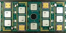
The Alpha 21164, also known by its code name, EV5, is a microprocessor developed and fabricated by Digital Equipment Corporation that implemented the Alpha instruction set architecture (ISA). It was introduced in January 1995, succeeding the Alpha 21064A as Digital's flagship microprocessor. It was succeeded by the Alpha 21264 in 1998.
History
First silicon of the Alpha 21164 was produced in February 1994, and the OpenVMS, Digital UNIX and Windows NT operating systems were successfully booted on it. It was sampled in late 1994 and was introduced in January 1995 at 266 MHz. A 300 MHz version was introduced in March 1995. The final Alpha 21164, a 333 MHz version, was announced on 2 October 1995, available in sample quantities. The Alpha 21164 was replaced by the Alpha 21164A as Digital's flagship microprocessor in 1996 when a 400 MHz version became available in volume quantities.
Users
Digital used the Alpha 21164 operating at various clock frequencies in their AlphaServer servers, AlphaStation workstations. Digital also used the Alpha 21164 in their Alpha VME 5/352 and Alpha VME 5/480 single board computers and AlphaPC 164 and AlphaPC 164LX motherboards. Alpha partner Cray Research used a 300 MHz Alpha 21164 in their T3E-600 supercomputer. Third parties such as DeskStation also built workstations using the Alpha 21164.
Performance
The 21164 continued the performance lead from the 275 MHz Alpha 21064A until the introduction of the Intel Pentium Pro in November 1995, when a 200 MHz version outperformed the 300 MHz 21164 on the SPECint95_base benchmark suite. The 21164 retained its floating-point performance lead. The 333 MHz 21164 introduce the following year outperformed the Pentium Pro, but it was later surpassed by the MIPS Technologies R10000 and then by the Hewlett-Packard PA-8000 in the same year.[1]
Description
The Alpha 21164 is a four-issue superscalar microprocessor capable of issuing a maximum of four instructions per clock cycle to four execution units: two integer and two floating-point. The integer pipeline is seven stages long, and the floating-point pipeline is ten stages long. The 21164 implemented a 43-bit virtual address and a 40-bit physical address. It was therefore capable of addressing 8 TB of virtual memory and 1 TB of physical memory.
Integer unit
The integer unit consisted of two integer pipelines and the integer register file. The two pipelines, the add pipeline and the multiply pipeline are not identical, each are responsible for executing different instructions, although both are capable of executing common add, logical, load, compare, and conditional move instructions. The multiply pipeline exclusively executes shift, store, and multiply instructions (in a non-pipelined multiplier). The add pipeline exclusively executes branch instructions.
Except for branch, conditional move, and multiply instructions, all other instructions begin and finish execution during stage five for a one cycle latency. Branch and conditional move instructions are executed during stage six so they can be issued with a compare instruction whose result they depend on.
The integer register file contained forty 64-bit registers, of which thirty-two are specified by the Alpha Architecture and eight are for use by PALcode as scratchpad memory. The register file has four read ports and two write ports evenly divided between the two integer pipelines.[2]
Floating-point unit
The floating-point unit consisted of two floating-point pipelines and the floating point register file. The two pipelines are not identical, one executed all floating-point instructions except for multiply, and the other executed only multiply instructions. Both pipelines have four stages. A non-pipelined floating-point divider is connected to the add pipeline. All floating-point instructions except for divide have four-cycle latency. Divides have variable latency that depends on whether the operation is being performed on single or on double precision floating-point numbers and numbers. Including overhead, single precision divides have a 15- to 31-cycle latency, whereas double precision divides have a 22- to 60-cycle latency.
Cache
The 21164 has three levels of cache, two on-die and one external and optional. The caches and the associated logic consisted of 7.2 million transistors.[3]
The primary cache is split into separate caches for instructions and data, referred to as the I-cache and D-cache respectively. They are 8 KB in size, direct-mapped and have a cache line size of 32 bytes. The D-cache is dual-ported, to improve performance, and is implemented by duplicating the cache twice. It uses a write-through write policy and an on-read allocation policy.
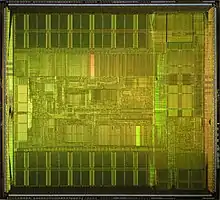
The secondary cache, known as the S-cache, is on-die and has a capacity of 96 KB. An on-die secondary cache was required as the 21164 required more bandwidth than an external secondary cache could supply in order to provide it with enough instructions and data.[4] The cache required two cycles to access due to its large area. To improve performance, the cache is pipelined. Another benefit of an on-die secondary cache was that it could be easily implemented as a multi-way cache, and as a result, the cache is three-way set associative, offering improved hit rates than direct-mapped caches.[5] The S-cache, due to the large physical area required, was implemented in two halves which flank the I-box, E-box, F-box and M-box. This was done so the cache could return data in two cycles.
The tertiary cache, known as the B-cache, is implemented with external SRAMs. The B-cache was optional and some systems using the Alpha 21164 did not have any. The B-cache could have a capacity of 1 to 64 MB, smaller capacities were not supported as they were rendered useless by the on-die S-cache.[6] It is direct-mapped, uses a write-back write policy and an on-write allocation policy. The B-cache is controlled by on-die external interface logic, unlike the 21064, which required an external cache controller. The B-cache could be built with asynchronous or synchronous SRAMs. The B-cache is accessed via the system bus.
External interface
The external interface is a 128-bit system bus. The system bus operates at a clock frequency that is 3 to 15 times lower than the internal clock frequency, or 20 to 100 MHz with an internal clock frequency 300 MHz. The system bus' clock signal is generated by the microprocessor.
Clock
The internal clock frequency is generated by dividing an external clock signal by two. The Alpha 21164 therefore requires an external clock signal of 600 MHz for a 300 MHz Alpha 21164.
Fabrication
The Alpha 21164 contains 9.3 million transistors on a die measuring 16.5 by 18.1 mm (299 mm2), which was close to the maximum limits of the process. The die was fabricated in Digital's fifth-generation complementary metal–oxide–semiconductor (CMOS) process, CMOS-5, a 0.50 μm process with four levels of aluminium interconnect.[7] The 21164 used a 3.3-volt (V) power supply. It dissipated 46 W at 266 MHz, 51 W at 300 MHz, 56 W at 333 MHz.
Package
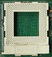
The Alpha 21164 is packaged in a 499-pin ceramic interstitial pin grid array (IPGA) measuring 57.40 by 57.40 mm. The package had a heat spreader with two studs to which the heat sink was bolted.
Derivatives
Alpha 21164 (EV56)
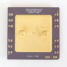
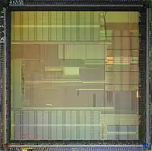
The Alpha 21164 was the basis of a further development code-named EV56. It was introduced as the Alpha 21164, but was originally known as the Alpha 21164A. It operated at clock frequencies of 366, 433, 500, 533, 566, 600 and 666 MHz.[8][9][10]
History
It was first described in October 1995 at the Microprocessor Forum. On 13 November 1995, Digital announced that samples would ship later in the month. The first version, operating at 366 MHz, was introduced in 1996. On 8 July 1996, Digital announced that a 433 MHz version was available and a 500 MHz version was sampling with volume quantities due in September 1996. The 433 MHz version was priced at $1,492 per unit in quantities of 1,000. The 600 MHz version was introduced on 31 March 1997, shipping in volume quantities. Samsung Electronics signed a deal with Digital in June 1996 to second source the Alpha 21164A and the company was the only one to fabricate the 666 MHz model. 366 to 500 MHz samples were introduced on 11 November 1996 with volume availability in 1997. The Alpha 21164A was fabricated at Digital's Hudson, Massachusetts and Samsung's Kihueng, South Korea fabrication plants.
Users of the Alpha 21164A included Cray Research, Digital, Network Appliance (now NetApp), and DeskStation. Cray Research used 450, 600 and 675 MHz Alpha 21164As in later models of their T3E supercomputer. Digital used the Alpha 21164A operating at various clock frequencies in their AlphaServers, AlphaStations, Celebris XL workstations and Digital Personal Workstations. NetApp used 400, 500 and 600 MHz Alpha 21164As in their storage systems. DeskStation used the Alpha 21164A in their Raptor Reflex workstations.
Description
The most notable change was the inclusion of Byte Word Extensions (BWX), an extension to the Alpha Architecture designed to improve byte and word accesses. These instructions are executed by the multiply pipeline. The Alpha 21164A contained 9.66 million transistors on a die measuring 14.4 mm by 14.5 mm, for a die area of 209 mm2.[11] Digital fabricated the die in their sixth generation CMOS process, CMOS-6, a 0.35 μm process with four layers of interconnect. Samsung fabricated the die in their 0.35 μm process with four layers of interconnect based on a 0.3 μm process they developed in early 1996. The Alpha 21164A used a 3.3 V power supply, dissipating 31.0 W at 366 MHz, 36.0 W at 433 MHz, 41.0 W at 500 MHz, 43.5 W at 533 MHz and 48.5 W at 600 MHz.
Alpha 21164PC (PCA56)
The Alpha 21164PC, also known as the PCA56, is a low-cost version of the Alpha 21164A introduced on 17 March 1997. The microprocessor was jointly developed by Digital and Mitsubishi Electric Corporation, and both companies fabricated the design. Mitsubishi later suspended the joint development agreement for future Alpha microprocessors with Digital in early 1998 and ceased to fabricate the Alpha 21164PC in mid-1998, exited the Alpha market because the economic conditions in the company's markets.[12][13]
The Alpha 21164PC operated at clock frequencies of 400, 466 and 533 MHz. Major changes are the omission of the S-cache, a larger I-cache, and the inclusion of Motion Video Instructions (MVI), an extension to the Alpha Architecture which introduced single instruction multiple data (SIMD) instructions for improving the performance of MPEG encoding. The S-cache was removed to reduce the transistor count, which reduced the die size and in turn, cost. The I-cache was doubled in capacity to 16 KB from 8 KB to compensate for the lack of S-cache, as the Alpha 21164 relied on the S-cache to complement the I-cache in order to provide enough bandwidth to achieve adequate performance. The amount of B-cache was limited to 512 KB to 4 MB, with 1 and 2 MB capacities also supported. The microprocessor uses a 43-bit virtual address and 33-bit physical address.
The Alpha 21164PC contained 3.5 million transistors on a die measuring 8.65 by 16.28 mm, for a die area of 141 mm2. Digital fabricated the die in the same process as the Alpha 21164, CMOS-5. The Alpha 21164PC was packaged in 413-pin IPGA measuring 49.78 by 49.78 mm. It used a 3.3 V power supply, dissipating 26.5 W at 400 MHz, 30.5 W at 466 MHz and 35.0 W at 533 MHz.
The Alpha 21164PC was used by Digital in their AlphaPC 164SX motherboard.
Alpha 21164PC (PCA57)
A derivative of the PCA56, the PCA57 was designed and fabricated by Samsung Electronics in a 0.28 μm CMOS process. The PCA57 was introduced in late 1998 and operated at clock frequencies of 533, 600 and 666 MHz. Improvements to the PCA56 microarchitecture included doubled I-cache and D-cache capacities: 32 KB and 16 KB respectively. The PCA57 contained 5.7 million transistors on a die measuring 6.7 mm by 15 mm, for a die area of 101 mm2. It operated on a 2.5 V power supply and dissipated 18 W at 533 MHz, 20 W at 600 MHz and 23 W at 666 MHz.
The PCA57 was used by Digital in its AlphaPC 164RX motherboard.
Chipsets
Digital and VLSI Technology developed chipsets for the 21164 and its derivatives. Digital also developed custom application-specific integrated circuit (ASICs) for use in the high-end models of their AlphaServer family such as the AlphaServer 8200 and 8400.
21171
The 21171, also known as Alcor, was the first chipset for the 21164, introduced in January 1995 alongside the microprocessor it supports. It was developed and fabricated by Digital. The 21171 is an upgraded DECchip 21071 modified to support the new system bus protocol the 21164 uses. It consisted of a control chip that contained the memory and PCI controllers, and four data slice chips that interfaced the 256-bit memory bus and PCI bus to the system bus. The 21171 provides a 64-bit wide PCI bus that runs at 33 MHz.
21172
The 21172, also known as Alcor2, was an updated 21171 that supported the 21164A.
Pyxis
The Pyxis chipset, also known as the 21174, supported the 21164A and 21164PC microprocessors. Unlike previous chipsets, it was designed for low-cost systems. As a result, it was a single-chip design packaged in a 474-contact ceramic ball grid array (CBGA) instead of multiple packages.[14] It was subsequently used in cost-sensitive applications such as entry-level workstations (Digital Personal Workstation a-Series) and motherboards such as the AlphaPC 164LX and 164SX. When it was introduced, the 21174 was priced at US$142 in quantities of 1,000.[15]
The 21174 contains a memory controller and PCI controller. The memory controller supported up to 512 MB of synchronous dynamic random access memory (SDRAM) and accesses it via a 128-bit memory bus. The memory can be either ECC or parity protected. The PCI controller provided a PCI or PCI-X bus.
Polaris
Polaris is a system controller developed by VLSI Technology for personal computers that supports the 21164A and 21164PC microprocessors. Polaris was announced on 16 June 1997.[16] It supports up to 768 MB of EDO DRAM or up to 512 MB of SDRAM. The memory is accessed via a 128-bit bus. It provides a 32-bit, 33 MHz PCI bus for I/O.
Users of Polaris included Digital, for its AlphaPC 164RX motherboard.
Notes
- Gwennap 1996
- Bowhill et al., "Circuit implementation of a 300-MHz 64-bit second-generation CMOS Alpha CPU", p. 124.
- Bowhill et al., "Circuit implementation of a 300-MHz 64-bit second-generation CMOS Alpha CPU", p. 111.
- Gwennap, "Digital Leads the Pack with 21164", p. 1.
- Gwennap, "Digital Leads the Pack with 21164", pp. 1–2.
- Gwennap, "Digital Leads the Pack with 21164".
- Bowhill, et al., "Circuit implementation of a 300-MHz 64-bit second-generation CMOS Alpha CPU", pp. 100–101.
- Alpha 21164 Microprocessor Data Sheet, August 1998, p. 113.
- Digital Semiconductor 21164 Alpha Microprocessor Product Brief, 31 March 1997, p. 2.
- "CCL: DEC Alpha 566 vs. 600 MHz"
- Bouchard, "Design objectives of the 0.35 μm Alpha 21164 Microprocessor", p. 3, 5.
- Foremski, "Mitsubishi steps back from Alpha".
- Foremski, "Mitsubishi Electric stops Alpha microprocessor manufacture".
- Schumann 1997
- Gwennap 1997
- VLSI Technology 1997
References
- Bouchard, Gregg. "Design objectives of the 0.35 μm Alpha 21164 Microprocessor". IEEE Hot Chips Symposium, August 1996, IEEE Computer Society.
- Bowhill, William J. et al. (1995). "Circuit Implementation of a 300-MHz 64-bit Second-generation CMOS Alpha CPU". Digital Technical Journal, Volume 7, Number 1, pp. 100–118.
- Edmondson, John H. et al. (1995). "Internal Organization of the Alpha 21164, a 300-MHz 64-bit Quad-issue CMOS RISC Microprocessor". Digital Technical Journal, Volume 7, Number 1, 1995. pp. 119–135.
- Edmondson, John H. et al. (1995). "Superscalar Instruction Execution in the 21164 Alpha Microprocessor". IEEE Micro. pp. 33–43.
- Foremski, Tom (10 February 1998). "Mitsubishi steps back from Alpha". Electronics Weekly.
- Foremski, Tom (10 July 1998). "Mitsubishi Electric stops Alpha microprocessor manufacture". Electronics Weekly.
- Gwennap, Linley (12 September 1994). "Digital Leads the Pack with 21164". Microprocessor Report, Volume 8, Number 12.
- Gwennap, Linley (8 July 1996). "Digital's 21164 Reaches 500 MHz". Microprocessor Report, Volume 10, Number 9.
- Gwennap, Linley (31 March 1997). "Digital's 21164PC Aimed at PC Market". Microprocessor Report, Volume 11, Number 4.
- Ryan, Bob (October 1994). "Alpha Rides High". Byte.
- Samsung Semiconductor, Inc. (11 November 1996). "Samsung Introduces 500MHz Alpha 21164 Microprocessor; First product resulting from the Digital/Samsung licensing agreement to begin mass production by Q2 1997 Archived 2012-10-11 at the Wayback Machine". Press release.
- Schumann, Reinhard C. (1997). "Design of the 21174 memory controller for Digital Personal Workstations" Archived 2008-09-06 at the Wayback Machine. Digital Technical Journal 9 (2): 57–70.
- VLSI Technology (16 June 1997). "Polaris, VLSI's New Alpha System Controller, Breaks the Gigabyte/Second Memory Transfer Barrier. End-Users Gain Full Performance on Alpha Systems". Press release.
- CCL Forums (25 March 1998). "DEC Alpha 566 vs. 600 MHz"
Further reading
- Bannon, P., Saito, Y. (1997). "The Alpha 21164PC microprocessor". Proceedings of Compcon '97, pp. 20–27.
- Bhandarkar, Dileep P. (1995). Alpha Architecture and Implementations. Digital Press.
- Carlson, D. et al. (1998). "A 667 MHz RISC microprocessor containing a 6.0 ns 64 b integer multiplier". ISSCC Digest of Technical Papers, pp. 294–295.
- Carlson, D.A.; Castelino, R.W.; Mueller, R.O. (November 1997). "Multimedia extensions for a 550-MHz RISC microprocessor". IEEE Journal of Solid-State Circuits 32 (11): pp. 1618–1624.
- Jain, A.K. et al. (1997). "1.38 cm2 550 MHz microprocessor with multimedia extensions". ISSCC Digest of Technical Papers, pp. 174–175, 451.
- Gronowski, Paul E. et al. (May 1998). "High-performance microprocessor design". IEEE Journal of Solid-State Circuits 33 (5): pp. 676–686.
- Kobayashi, S. et al. (1997). "A 550 MHz Alpha microprocessor targeted at PC applications". Proceedings of the 1997 International Symposium on VLSI Technology, Systems, and Applications, pp. 203–207.