Anderson's rule
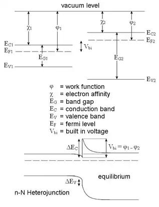
Anderson's rule is used for the construction of energy band diagrams of the heterojunction between two semiconductor materials. Anderson's rule states that when constructing an energy band diagram, the vacuum levels of the two semiconductors on either side of the heterojunction should be aligned (at the same energy).[1]

It is also referred to as the electron affinity rule, and is closely related to the Schottky–Mott rule for metal–semiconductor junctions.
Anderson's rule was first described by R. L. Anderson in 1960.[2]
Constructing energy band diagrams
| Eg (eV) | χ (eV) | |
|---|---|---|
| GaAs | 1.43 | 4.07 |
| AlAs | 2.16 | 2.62 |
| GaP | 2.21 | 4.3 |
| InAs | .36 | 4.9 |
| InP | 1.35 | 4.35 |
| Si | 1.12 | 4.05 |
| Ge | .66 | 4.0 |
Once the vacuum levels are aligned it is possible to use the electron affinity and band gap values for each semiconductor to calculate the conduction band and valence band offsets.[4] The electron affinity (usually given by the symbol in solid state physics) gives the energy difference between the lower edge of the conduction band and the vacuum level of the semiconductor. The band gap (usually given the symbol ) gives the energy difference between the lower edge of the conduction band and the upper edge of the valence band. Each semiconductor has different electron affinity and band gap values. For semiconductor alloys it may be necessary to use Vegard's law to calculate these values.
Once the relative positions of the conduction and valence bands for both semiconductors are known, Anderson's rule allows the calculation of the band offsets of both the valence band () and the conduction band (). After applying Anderson's rule and discovering the bands' alignment at the junction, Poisson’s equation can then be used to calculate the shape of the band bending in the two semiconductors.
Example: straddling gap
Consider a heterojunction between semiconductor 1 and semiconductor 2. Suppose the conduction band of semiconductor 2 is closer to the vacuum level than that of semiconductor 1. The conduction band offset would then be given by the difference in electron affinity (energy from upper conducting band to vacuum level) of the two semiconductors:
Next, suppose that the band gap of semiconductor 2 is large enough that the valence band of semiconductor 1 lies at a higher energy than that of semiconductor 2. Then the valence band offset is given by:
Limitations of Anderson's rule
In real semiconductor heterojunctions, Anderson's rule fails to predict actual band offsets. In Anderson's idealized model the materials are assumed to behave as they would in the limit of a large vacuum separation, yet where the vacuum separation is taken to zero. It is that assumption that involves the use of the vacuum electron affinity parameter, even in a solidly filled junction where there is no vacuum. Much like with the Schottky–Mott rule, Anderson's rule ignores the real chemical bonding effects that occur with a small or nonexistent vacuum separation: interface states which may have a very large electrical polarization and defect states, dislocations and other perturbations caused by imperfect crystal lattice matches.
To try to improve the accuracy of Anderson's rule, various models have been proposed. The common anion rule guesses that, since the valence band is related to anionic states, materials with the same anions should have very small valence band offsets. Tersoff[5] proposed the presence of a dipole layer due to induced gap states, by analogy to the metal-induced gap states in a metal–semiconductor junction. Practically, heuristic corrections to Anderson's rule have found success in specific systems, such as the 60:40 rule used for the GaAs/AlGaAs system.[6]
References
- Borisenko, V. E. and Ossicini, S. (2004). What is What in the Nanoworld: A Handbook on Nanoscience and Nanotechnology. Germany: Wiley-VCH.
- Anderson, R. L. (1960). "Germanium-Gallium Arsenide Heterojunctions [Letter to the Editor]". IBM Journal of Research and Development. 4 (3): 283–287. doi:10.1147/rd.43.0283. ISSN 0018-8646.
- Pallab, Bhattacharya (1997), Semiconductor Optoelectronic Devices, Prentice Hall, ISBN 0-13-495656-7
- Davies, J. H., (1997). The Physics of Low-Dimensional Semiconductors. UK: Cambridge University Press.
- J. Tersoff (1984). "Theory of semiconductor heterojunctions: The role of quantum dipoles". Physical Review B. 30 (8): 4874–4877. Bibcode:1984PhRvB..30.4874T. doi:10.1103/PhysRevB.30.4874.
- Debbar, N.; Biswas, Dipankar; Bhattacharya, Pallab (1989). "Conduction-band offsets in pseudomorphic InxGa1-xAs/Al0.2Ga0.8As quantum wells (0.07≤x≤0.18) measured by deep-level transient spectroscopy". Physical Review B. 40 (2): 1058–1063. Bibcode:1989PhRvB..40.1058D. doi:10.1103/PhysRevB.40.1058. PMID 9991928.