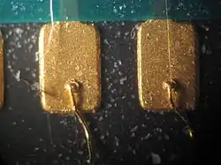
Contact pad
Contact pads or bond pads are small, conductive surface areas of a printed circuit board (PCB) or die of an integrated circuit. They are often made of gold, copper, or aluminum and measure mere micrometres wide. Pads are positioned on the edges of die, to facilitate connections without shorting. Contact pads exist to provide a larger surface area for connections to a microchip or PCB, allowing for the input and output of data and power.

Possible methods of connecting contact pads to a system include soldering, wirebonding, or flip chip mounting.
Contact pads are created alongside a chip's functional structure during the photolithography steps of the fabrication process, and afterwards they are tested. During the test process, contact pads are probed with the needles of a probe card on Automatic Test Equipment in order to check for faults via electrical resistance.
Further reading
- Kraig Mitzner, Complete PCB Design Using OrCAD Capture and PCB Editor, Newnes, 2009 ISBN 0-08-094354-3.
- Jing Li, Evaluation and Improvement of the Robustness of a PCB Pad in a Lead-free Environment, ProQuest, 2007 ISBN 0-549-32110-1.
- Deborah Lea, Fredirikus Jonck, Christopher Hunt, Solderability Measurements of PCB Pad Finishes and Geometries, National Physical Laboratory, 2001 OCLC 59500348.