Charge modulation spectroscopy
Charge modulation Spectroscopy is an electro-optical spectroscopy technique tool.[1] It is used to study the charge carrier behavior of Organic field-effect transistor. It measures the charge introduced optical transmission variation[2][3] by directly probing the accumulation charge at the burning interface of semiconductor and dielectric layer[4] where the conduction channel forms.

Principles
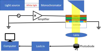
Unlike ultraviolet–visible spectroscopy which measures absorbance, charge modulation spectroscopy measures the charge introduced optical transmission variation. In other words, it reveals the new features in optical transmission introduced by charges. In this setup, there are mainly four components: lamp, monochromator, photodetector and lock-in amplifier. Lamp and monochromator are used for generating and selecting the wavelength. The selected wavelength passes through the transistor, and the transmitted light is recorded by the Photodiode. When the signal to noise ratio is very low, the signal can be modulated and recovered with a Lock-in amplifier.
In the experiment, a direct current plus an alternating current bias are applied to the organic field-effect transistor. Charge carries accumulate at the interface between the dielectric and the semiconductor (usually a few nanometers[5]). With the appearance of the accumulation charge, the intensity of the transmitted light changes. The variation of the light intensity (§ Bleaching and Charge absorption signal) is then collected though the photodetector and lock-in amplifier. The charge modulation frequency is given to Lock-in amplifier as the reference.
Modulate charge at the organic field-effect transistor

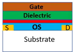
There are four typically Organic field-effect transistor architectures:[6] Top-gate, bottom-contacts; bottom-gate, top-contacts; bottom-gate, bottom-contacts; top-gate, top-contact.
In order to create the accumulation charge layer, a positive/negative direct current voltage is applied to the gate of the organic field-effect transistor (positive for the P type transistor, negative for the N type transistor).[7] In order to modulate the charge, an AC voltage is given between the gate and source. It is important to notice that only mobile charge can follow the modulation and that the modulation frequency given to lock-in amplifier has to be synchronous.
Charge modulation spectra
The charge modulation spectroscopy signal can be defined as the differential transmission divided by the total transmission . By modulating the mobile carriers, an increase transmission and decrease transmission features could be both observed.[8] The former relates to the bleaching and the latter to the charge absorption and electrically induced absorption (electro-absorption). The charge modulation spectroscopy spectra is an overlap of charge-induced and electro-absorption features. In transistors, the electro-absorption is more significant during the high voltage drop.[9] There are several ways to identify the electro-absorption contribution, such as get the second harmonic , or probe it at the depletion region.
Bleaching and charge absorption
When the accumulation charge carrier removes the ground state of the neutral polymer, there is more transmission in the ground state. This is called bleaching . With the excess hole or electrons at the polymer, there will be new transitions at low energy levels, therefore the transmission intensity is reduced , this is related to charge absorption.[1]
Electro-absorption
The electro-absorption is a type of Stark effect in the neutral polymer,[10] it is predominant at the electrode edge since there is a strong voltage drop. Electro-absorption can be observed from the second harmonic charge modulation spectroscopy spectra.[9]
Charge modulation microscopy
Charge modulation microscopy is a new technology which combines the confocal microscopy with charge modulation spectroscopy.[11] Unlike the charge modulation spectroscopy which is focused on the whole transistor, the charge modulation microscopy give us the local spectra and map. Thanks for this technology, the channel spectra and electrode spectra can be obtained individually. A more local dimension of charge modulation spectra (around submicrometer) can be observed without a significant Electro-absorption feature. Of course, this depends on the resolution of the optical microscopy.
The high resolution of charge modulation microscopy allows mapping of the charge carrier distribution at the active channel of the organic field-effect transistor.[9] In other words, a functional carrier morphology can be observed. It is well known that the local carrier density can be related to the polymer microstructure. Based on Density functional theory calculations, a polarized charge modulation microscopy can selectively map the charge transport associated with a relative direction of the transition dipole moment.[12] The local direction can be correlated to the orientational order of polymer domains.[13] More ordered domains show a high carrier mobility of the organic field-effect transistor device.
See also
References
- Caironi, Mario; Bird, Matt; Fazzi, Daniele; Chen, Zhihua; Di Pietro, Riccardo; Newman, Christopher; Facchetti, Antonio; Sirringhaus, Henning (9 September 2011). "Very Low Degree of Energetic Disorder as the Origin of High Mobility in an n-channel Polymer Semiconductor". Advanced Functional Materials. 21 (17): 3371–3381. doi:10.1002/adfm.201100592. S2CID 95644182.
- Sirringhaus, H.; Brown, P. J.; Friend, R. H.; Nielsen, M. M.; Bechgaard, K.; Langeveld-Voss, B. M. W.; Spiering, A. J. H.; Janssen, R. A. J.; Meijer, E. W.; Herwig, P.; de Leeuw, D. M. (October 1999). "Two-dimensional charge transport in self-organized, high-mobility conjugated polymers". Nature. 401 (6754): 685–688. Bibcode:1999Natur.401..685S. doi:10.1038/44359. S2CID 4387286.
- Brown, Peter J.; Sirringhaus, Henning; Harrison, Mark; Shkunov, Maxim; Friend, Richard H. (12 March 2001). "Optical spectroscopy of field-induced charge in self-organized high mobility poly(3-hexylthiophene)". Physical Review B. 63 (12): 125204. Bibcode:2001PhRvB..63l5204B. doi:10.1103/physrevb.63.125204.
- Large area and flexible electronics. Wiley-VCH. 2015-05-04. ISBN 9783527336395.
- Bässler, H. (1 January 1993). "Charge Transport in Disordered Organic Photoconductors a Monte Carlo Simulation Study". Physica Status Solidi B. 175 (1): 15–56. Bibcode:1993PSSBR.175...15B. doi:10.1002/pssb.2221750102.
- Marder, Seth R.; Bredas, Jean-Luc (2016-01-29). The WSPC reference on organic electronics : organic semiconductors (in 2 volumes). ISBN 9789814699228.
- Organic thin film transistor integration : a hybrid approach. Wiley-VCH. 2011-03-21. ISBN 978-3527634453.
- Zhao, N.; Noh, Y.-Y.; Chang, J.-F.; Heeney, M.; McCulloch, I.; Sirringhaus, H. (5 October 2009). "Polaron Localization at Interfaces in High-Mobility Microcrystalline Conjugated Polymers". Advanced Materials. 21 (37): 3759–3763. Bibcode:2009AdM....21.3759Z. doi:10.1002/adma.200900326. S2CID 95098433.
- Chin, Xin Yu; Pace, Giuseppina; Soci, Cesare; Caironi, Mario (2017). "Ambipolar charge distribution in donor–acceptor polymer field-effect transistors". Journal of Materials Chemistry C. 5 (3): 754–762. doi:10.1039/c6tc05033f.
- Chemla, D. S.; Damen, T. C.; Miller, D. A. B.; Gossard, A. C.; Wiegmann, W. (15 May 1983). "Electroabsorption by Stark effect on room‐temperature excitons in GaAs/GaAlAs multiple quantum well structures". Applied Physics Letters. 42 (10): 864–866. Bibcode:1983ApPhL..42..864C. doi:10.1063/1.93794.
- Sciascia, Calogero; Martino, Nicola; Schuettfort, Torben; Watts, Benjamin; Grancini, Giulia; Antognazza, Maria Rosa; Zavelani-Rossi, Margherita; McNeill, Christopher R.; Caironi, Mario (16 November 2011). "Sub-Micrometer Charge Modulation Microscopy of a High Mobility Polymeric n-Channel Field-Effect Transistor". Advanced Materials. 23 (43): 5086–5090. Bibcode:2011AdM....23.5086S. doi:10.1002/adma.201102410. PMID 21989683. S2CID 205241797.
- Fazzi, Daniele; Caironi, Mario (2015). "Multi-length-scale relationships between the polymer molecular structure and charge transport: the case of poly-naphthalene diimide bithiophene". Physical Chemistry Chemical Physics. 17 (14): 8573–8590. Bibcode:2015PCCP...17.8573F. doi:10.1039/c5cp00523j. PMID 25740386.
- Martino, Nicola; Fazzi, Daniele; Sciascia, Calogero; Luzio, Alessandro; Antognazza, Maria Rosa; Caironi, Mario (13 May 2014). "Mapping Orientational Order of Charge-Probed Domains in a Semiconducting Polymer". ACS Nano. 8 (6): 5968–5978. doi:10.1021/nn5011182. hdl:11858/00-001M-0000-0024-A80B-8. PMID 24815931.
Further reading
- Ziffer, Mark E.; Mohammed, Joseph C.; Ginger, David S. (20 May 2016). "Electroabsorption Spectroscopy Measurements of the Exciton Binding Energy, Electron–Hole Reduced Effective Mass, and Band Gap in the Perovskite CH3 NH3PbI3". ACS Photonics. 3 (6): 1060–1068. doi:10.1021/acsphotonics.6b00139.
- Uchida, R.; Yada, H.; Makino, M.; Matsui, Y.; Miwa, K.; Uemura, T.; Takeya, J.; Okamoto, H. (4 March 2013). "Charge modulation infrared spectroscopy of rubrene single-crystal field-effect transistors". Applied Physics Letters. 102 (9): 093301. Bibcode:2013ApPhL.102i3301U. doi:10.1063/1.4794055.
- Liu, Chuan; Huang, Kairong; Park, Won-Tae; Li, Minmin; Yang, Tengzhou; Liu, Xuying; Liang, Lijuan; Minari, Takeo; Noh, Yong-Young (2017). "A unified understanding of charge transport in organic semiconductors: the importance of attenuated delocalization for the carriers". Materials Horizons. 4 (4): 608–618. doi:10.1039/C7MH00091J.