Crossbar latch
Crossbar Latch is a technology devised by Phillip Kuekes of HP Labs in 2001 (with a US patent being granted in 2003[1]), that Hewlett-Packard believes might replace transistors in various applications. This would enable the creation of integrated circuits composed solely of memristors, which, according to the patent, might be easier and less expensive to create. HP Labs stated that memristors could someday replace transistors in the same way that transistors replaced vacuum tubes.[2]
Details
The crossbar was introduced by HP Labs scientists in the Journal of Applied Physics, which provides a basis for constructing logic gates using memristors. The crossbar latch consists of a signal line crossed by two control lines. Depending on the voltages sent down the various lines, it can simulate the action of the three major logic gates: AND, OR and NOT.
The abstract of the patent is as follows:
"A molecular crossbar latch is provided, comprising two control wires and a signal wire that crosses the two control wires at a non-zero angle to thereby form a junction with each control wire. Each junction forms a switch and the junction has a functional dimension in nanometers. The signal wire selectively has at least two different voltage states, ranging from a 0 state to a 1 state, wherein there is an asymmetry with respect to the direction of current flow from the signal wire through one junction compared to another junction such that current flowing through one junction into (out of) the signal wire can open (close) while current flowing through the other junction out of (into) the signal wire can close (open) the switch, and wherein there is a voltage threshold for switching between an open switch and a closed switch. Further, methods are provided for latching logic values onto nanowires in a logic array, for inverting a logic value, and for restoring a voltage value of a signal in a nano-scale wire. Invented by Phillip J Kuekes."
— U.S. patent 6,586,965[3]
Applications in arithmetic processing

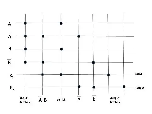
Greg Snider of Hewlett-Packard created this application, which uses crossbar latches to imitate the functionality of a half adder, which is the foundation of modern computing systems. [4] A crossbar tile is created in this application from a layer of horizontal row wires and a layer of vertical column wires, with memristor or similar materials sandwiched between the horizontal and vertical wire layers. Each crossbar tile intersection or junction can be configured to be in a high-resistance state with little or no current flowing between the horizontal and vertical wires, or in a low-resistance state with current flowing. Fig. 1 illustrates the configuration of a half-adder using a crossbar tile, as taught by Snider, with the nodes identifying junctions of the crossbar tile configured as low-resistance states. By setting different logic inputs A, NOT A, B, and NOT B to different row wires this configuration produces the sum and carry outputs typical for a half-adder. Connections between multiple half-adders may then be used to form full adders in accordance with conventional arithmetic architectures.
Applications of crossbar latch in neuromorphics
Crossbar latches have been suggested as components of neuromorphic computing systems. One implementation of this is in the form of a neural network formed from nanowires as discussed in a patent by Greg Snider of Hewlett-Packard.[5]
See also
References
- "Researchers Find that the 'Crossbar Latch' Can Replace Transistors and Improve Processing Power". AZoNano.com. 2005-04-21. Retrieved 2021-12-23.
- Singer, Michael. "HP's "Crossbar Latch' to Replace Transistors?". InternetNews.com. InternetNews.com. Retrieved 8 May 2015.
- "U.S. Patent 6,586,965".
- "U.S. Patent 7,203,789".
- "U.S. Patent 7,359,888".
External links
- U.S. Patent 6,586,965
- Research could send transistors the way of the vacuum tube (HP Press Release)
- HP claims molecular computing breakthrough (ComputerWorld)