DDR SDRAM
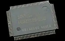
Double Data Rate Synchronous Dynamic Random-Access Memory (DDR SDRAM) is a double data rate (DDR) synchronous dynamic random-access memory (SDRAM) class of memory integrated circuits used in computers. DDR SDRAM, also retroactively called DDR1 SDRAM, has been superseded by DDR2 SDRAM, DDR3 SDRAM, DDR4 SDRAM and DDR5 SDRAM. None of its successors are forward or backward compatible with DDR1 SDRAM, meaning DDR2, DDR3, DDR4 and DDR5 memory modules will not work on DDR1-equipped motherboards, and vice versa.
| Computer memory and data storage types |
|---|
| Volatile |
| Non-volatile |
 Comparison of DDR modules for desktop PCs (DIMM). | |
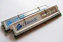
.jpg.webp) Front and back of a 1GB DDR-400 RAM module for desktop PCs (DIMM) | |
| Developer | |
|---|---|
| Type | Synchronous dynamic random-access memory |
| Generations | |
| Release date |
|
| Specifications | |
| Voltage |
|
Compared to single data rate (SDR) SDRAM, the DDR SDRAM interface makes higher transfer rates possible through more strict control of the timing of the electrical data and clock signals. Implementations often have to use schemes such as phase-locked loops and self-calibration to reach the required timing accuracy.[4][5] The interface uses double pumping (transferring data on both the rising and falling edges of the clock signal) to double data bus bandwidth without a corresponding increase in clock frequency. One advantage of keeping the clock frequency low is that it reduces the signal integrity requirements on the circuit board connecting the memory to the controller. The name "double data rate" refers to the fact that a DDR SDRAM with a certain clock frequency achieves nearly twice the bandwidth of a SDR SDRAM running at the same clock frequency, due to this double pumping.
With data being transferred 64 bits at a time, DDR SDRAM gives a transfer rate (in bytes/s) of (memory bus clock rate) × 2 (for dual rate) × 64 (number of bits transferred) / 8 (number of bits/byte). Thus, with a bus frequency of 100 MHz, DDR SDRAM gives a maximum transfer rate of 1600 MB/s.
History

In the late 1980s IBM had built DRAMs using a dual-edge clocking feature and presented their results at the International Solid-State Circuits Convention in 1990.[6][7]
Samsung demonstrated the first DDR memory prototype in 1997,[1] and released the first commercial DDR SDRAM chip (64 Mbit) in June 1998,[8][2][3] followed soon after by Hyundai Electronics (now SK Hynix) the same year.[9] The development of DDR began in 1996, before its specification was finalized by JEDEC in June 2000 (JESD79).[10] JEDEC has set standards for the data rates of DDR SDRAM, divided into two parts. The first specification is for memory chips, and the second is for memory modules. The first retail PC motherboard using DDR SDRAM was released in August 2000.[11]
Specification
.jpg.webp)


Modules
To increase memory capacity and bandwidth, chips are combined on a module. For instance, the 64-bit data bus for DIMM requires eight 8-bit chips, addressed in parallel. Multiple chips with common address lines are called a memory rank. The term was introduced to avoid confusion with chip internal rows and banks. A memory module may bear more than one rank. The term sides would also be confusing because it incorrectly suggests the physical placement of chips on the module. All ranks are connected to the same memory bus (address + data). The chip select signal is used to issue commands to specific rank.
Adding modules to the single memory bus creates additional electrical load on its drivers. To mitigate the resulting bus signaling rate drop and overcome the memory bottleneck, new chipsets employ the multi-channel architecture.
| Name | Chip | Bus | Timings | Voltage (V) | ||||||
|---|---|---|---|---|---|---|---|---|---|---|
| Standard | Type | Module | Clock rate (MHz) | Cycle time (ns)[12] | Clock rate (MHz) | Transfer rate (MT/s) | Bandwidth (MB/s) | CL-TRCD-TRP | CAS latency (ns) | |
| DDR-200 | PC-1600 | 100 | 10 | 100 | 200 | 1600 | 2-2-2 | 20 | 2.5±0.2 | |
| DDR-266 | PC-2100 | 133+1⁄3 | 7.5 | 133+1⁄3 | 266.67 | 2133+1⁄3 | 2.5-3-3 | 18.75 | ||
| DDR-333 | PC-2700 | 166+2⁄3 | 6 | 166+2⁄3 | 333+1⁄3 | 2666+2⁄3 | 2.5-3-3 | 15 | ||
| DDR-400 | A | PC-3200 | 200 | 5 | 200 | 400 | 3200 | 2.5-3-3 | 12.5 | 2.6±0.1 |
| B | 3-3-3 | 15 | ||||||||
| C | 3-4-4 | 15 | ||||||||
Note: All items listed above are specified by JEDEC as JESD79F.[13] All RAM data rates in-between or above these listed specifications are not standardized by JEDEC – often they are simply manufacturer optimizations using tighter tolerances or overvolted chips. The package sizes in which DDR SDRAM is manufactured are also standardized by JEDEC.
There is no architectural difference between DDR SDRAM modules. Modules are instead designed to run at different clock frequencies: for example, a PC-1600 module is designed to run at 100 MHz, and a PC-2100 is designed to run at 133 MHz. A module's clock speed designates the data rate at which it is guaranteed to perform, hence it is guaranteed to run at lower (underclocking) and can possibly run at higher (overclocking) clock rates than those for which it was made.[14]
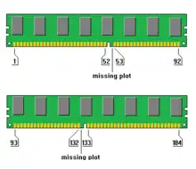
DDR SDRAM modules for desktop computers, dual in-line memory modules (DIMMs), have 184 pins (as opposed to 168 pins on SDRAM, or 240 pins on DDR2 SDRAM), and can be differentiated from SDRAM DIMMs by the number of notches (DDR SDRAM has one, SDRAM has two). DDR SDRAM for notebook computers, SO-DIMMs, have 200 pins, which is the same number of pins as DDR2 SO-DIMMs. These two specifications are notched very similarly and care must be taken during insertion if unsure of a correct match. Most DDR SDRAM operates at a voltage of 2.5 V, compared to 3.3 V for SDRAM. This can significantly reduce power consumption. Chips and modules with the DDR-400/PC-3200 standard have a nominal voltage of 2.6 V.
JEDEC Standard No. 21–C defines three possible operating voltages for 184 pin DDR, as identified by the key notch position relative to its centreline. Page 4.5.10-7 defines 2.5V (left), 1.8V (centre), TBD (right), while page 4.20.5–40 nominates 3.3V for the right notch position. The orientation of the module for determining the key notch position is with 52 contact positions to the left and 40 contact positions to the right.
Increasing the operating voltage slightly can increase maximum speed but at the cost of higher power dissipation and heating, and at the risk of malfunctioning or damage.
- Capacity
- Number of DRAM devices
- The number of chips is a multiple of 8 for non-ECC modules and a multiple of 9 for ECC modules. Chips can occupy one side (single sided) or both sides (dual sided) of the module. The maximal number of chips per DDR module is 36 (9×4) for ECC and 32 (8x4) for non-ECC.
- ECC vs non-ECC
- Modules that have error-correcting code are labeled as ECC. Modules without error correcting code are labeled non-ECC.
- Timings
- CAS latency (CL), clock cycle time (tCK), row cycle time (tRC), refresh row cycle time (tRFC), row active time (tRAS).
- Buffering
- Registered (or buffered) vs unbuffered.
- Packaging
- Typically DIMM or SO-DIMM.
- Power consumption
- A test with DDR and DDR2 RAM in 2005 found that average power consumption appeared to be of the order of 1–3 W per 512 MB module; this increases with clock rate and when in use rather than idling.[15] A manufacturer has produced calculators to estimate the power used by various types of RAM.[16]
Module and chip characteristics are inherently linked.
Total module capacity is a product of one chip's capacity and the number of chips. ECC modules multiply it by 8⁄9 because they use 1 bit per byte (8 bits) for error correction. A module of any particular size can therefore be assembled either from 32 small chips (36 for ECC memory), or 16(18) or 8(9) bigger ones.
DDR memory bus width per channel is 64 bits (72 for ECC memory). Total module bit width is a product of bits per chip and number of chips. It also equals number of ranks (rows) multiplied by DDR memory bus width. Consequently, a module with a greater number of chips or using ×8 chips instead of ×4 will have more ranks.
| Module size (GB) | Number of chips | Chip size (Mbit) | Chip organization | Number of ranks |
|---|---|---|---|---|
| 1 | 36 | 256 | 64M×4 | 2 |
| 1 | 18 | 512 | 64M×8 | 2 |
| 1 | 18 | 512 | 128M×4 | 1 |
This example compares different real-world server memory modules with a common size of 1 GB. One should definitely be careful buying 1 GB memory modules, because all these variations can be sold under one price position without stating whether they are ×4 or ×8, single- or dual-ranked.
There is a common belief that number of module ranks equals number of sides. As above data shows, this is not true. One can also find 2-side/1-rank modules. One can even think of a 1-side/2-rank memory module having 16(18) chips on single side ×8 each, but it is unlikely such a module was ever produced.
Chip characteristics

- DRAM density
- Size of the chip is measured in megabits. Most motherboards recognize only 1 GB modules if they contain 64M×8 chips (low density). If 128M×4 (high density) 1 GB modules are used, they most likely will not work. The JEDEC standard allows 128M×4 only for registered modules designed specifically for servers, but some generic manufacturers do not comply.[17]
- Organization
- The notation like 64M×4 means that the memory matrix has 64 million (the product of banks x rows x columns) 4-bit storage locations. There are ×4, ×8, and ×16 DDR chips. The ×4 chips allow the use of advanced error correction features like Chipkill, memory scrubbing and Intel SDDC in server environments, while the ×8 and ×16 chips are somewhat less expensive. x8 chips are mainly used in desktops/notebooks but are making an entry into the server market. There are normally 4 banks and only one row can be active in each bank.
Double data rate (DDR) SDRAM specification
From Ballot JCB-99-70, and modified by numerous other Board Ballots, formulated under the cognizance of Committee JC-42.3 on DRAM Parametrics.
Standard No. 79 Revision Log:
- Release 1, June 2000
- Release 2, May 2002
- Release C, March 2003 – JEDEC Standard No. 79C.[18]
"This comprehensive standard defines all required aspects of 64Mb through 1Gb DDR SDRAMs with X4/X8/X16 data interfaces, including features, functionality, ac and dc parametrics, packages and pin assignments. This scope will subsequently be expanded to formally apply to x32 devices, and higher density devices as well."
Organization
PC3200 is DDR SDRAM designed to operate at 200 MHz using DDR-400 chips with a bandwidth of 3,200 MB/s. Because PC3200 memory transfers data on both the rising and falling clock edges, its effective clock rate is 400 MHz.
1 GB PC3200 non-ECC modules are usually made with 16 512 Mbit chips, 8 on each side (512 Mbits × 16 chips) / (8 bits (per byte)) = 1,024 MB. The individual chips making up a 1 GB memory module are usually organized as 226 8-bit words, commonly expressed as 64M×8. Memory manufactured in this way is low-density RAM and is usually compatible with any motherboard specifying PC3200 DDR-400 memory.[19]
Generations
DDR (DDR1) was superseded by DDR2 SDRAM, which had modifications for a higher clock frequency and again doubled throughput, but operates on the same principle as DDR. Competing with DDR2 was Rambus XDR DRAM. DDR2 dominated due to cost and support factors. DDR2 was in turn superseded by DDR3 SDRAM, which offered higher performance for increased bus speeds and new features. DDR3 has been superseded by DDR4 SDRAM, which was first produced in 2011 and whose standards were still in flux (2012) with significant architectural changes.
DDR's prefetch buffer depth is 2 (bits), while DDR2 uses 4. Although the effective clock rates of DDR2 are higher than DDR, the overall performance was not greater in the early implementations, primarily due to the high latencies of the first DDR2 modules. DDR2 started to be effective by the end of 2004, as modules with lower latencies became available.[20]
Memory manufacturers stated that it was impractical to mass produce DDR1 memory with effective transfer rates in excess of 400 MHz (i.e. 400 MT/s and 200 MHz external clock) due to internal speed limitations. DDR2 picks up where DDR1 leaves off, utilizing internal clock rates similar to DDR1, but is available at effective transfer rates of 400 MHz and higher. DDR3 advances extended the ability to preserve internal clock rates while providing higher effective transfer rates by again doubling the prefetch depth.
The DDR4 SDRAM is a high-speed dynamic random-access memory internally configured as 16 banks, 4 bank groups with 4 banks for each bank group for ×4/×8 and 8 banks, 2 bank groups with 4 banks for each bank group for ×16 DRAM. The DDR4 SDRAM uses an 8n prefetch architecture to achieve high-speed operation. The 8n prefetch architecture is combined with an interface designed to transfer two data words per clock cycle at the I/O pins. A single read or write operation for the DDR4 SDRAM consists of a single 8n-bit-wide 4-clock data transfer at the internal DRAM core and 8 corresponding n-bit-wide half-clock-cycle data transfers at the I/O pins.[21]
RDRAM was a particularly expensive alternative to DDR SDRAM, and most manufacturers dropped its support from their chipsets. DDR1 memory's prices substantially increased from Q2 2008, while DDR2 prices declined. In January 2009, 1 GB DDR1 was 2–3 times more expensive than 1 GB DDR2.
| Name | Release year |
Chip | Bus | Voltage (V) |
Pins | |||||||
|---|---|---|---|---|---|---|---|---|---|---|---|---|
| Gen | Standard | Clock rate (MHz) |
Cycle time (ns) |
Pre- fetch |
Clock rate (MHz) |
Transfer rate (MT/s) |
Bandwidth (MB/s) |
DIMM | SO- DIMM |
Micro- DIMM | ||
| DDR | DDR-200 | 1998 | 100 | 10 | 2n | 100 | 200 | 1600 | 2.5 | 184 | 200 | 172 |
| DDR-266 | 133 | 7.5 | 133 | 266 | 2133+1⁄3 | |||||||
| DDR-333 | 166+2⁄3 | 6 | 166+2⁄3 | 333 | 2666+2⁄3 | |||||||
| DDR-400 | 200 | 5 | 200 | 400 | 3200 | 2.6 | ||||||
| DDR2 | DDR2-400 | 2003 | 100 | 10 | 4n | 200 | 400 | 3200 | 1.8 | 240 | 200 | 214 |
| DDR2-533 | 133+1⁄3 | 7.5 | 266+2⁄3 | 533+1⁄3 | 4266+2⁄3 | |||||||
| DDR2-667 | 166+2⁄3 | 6 | 333+1⁄3 | 666+2⁄3 | 5333+1⁄3 | |||||||
| DDR2-800 | 200 | 5 | 400 | 800 | 6400 | |||||||
| DDR2-1066 | 266+2⁄3 | 3.75 | 533+1⁄3 | 1066+2⁄3 | 8533+1⁄3 | |||||||
| DDR3 | DDR3-800 | 2007 | 100 | 10 | 8n | 400 | 800 | 6400 | 1.5/1.35 | 240 | 204 | 214 |
| DDR3-1066 | 133+1⁄3 | 7.5 | 533+1⁄3 | 1066+2⁄3 | 8533+1⁄3 | |||||||
| DDR3-1333 | 166+2⁄3 | 6 | 666+2⁄3 | 1333+1⁄3 | 10600+2⁄3 | |||||||
| DDR3-1600 | 200 | 5 | 800 | 1600 | 12800 | |||||||
| DDR3-1866 | 233+1⁄3 | 4.29 | 933+1⁄3 | 1866+2⁄3 | 14933+1⁄3 | |||||||
| DDR3-2133 | 266+2⁄3 | 3.75 | 1066+2⁄3 | 2133+1⁄3 | 17066+2⁄3 | |||||||
| DDR4 | DDR4-1600 | 2014 | 200 | 5 | 8n | 800 | 1600 | 12800 | 1.2/1.05 | 288 | 260 | - |
| DDR4-1866 | 233+1⁄3 | 4.29 | 933+1⁄3 | 1866+2⁄3 | 14933+1⁄3 | |||||||
| DDR4-2133 | 266+2⁄3 | 3.75 | 1066+2⁄3 | 2133+1⁄3 | 17066+2⁄3 | |||||||
| DDR4-2400 | 300 | 3+1⁄3 | 1200 | 2400 | 19200 | |||||||
| DDR4-2666 | 333+1⁄3 | 3 | 1333+1⁄3 | 2666+2⁄3 | 21333+1⁄3 | |||||||
| DDR4-2933 | 366+2⁄3 | 2.73 | 1466+2⁄3 | 2933+1⁄3 | 23466+2⁄3 | |||||||
| DDR4-3200 | 400 | 2.5 | 1600 | 3200 | 25600 | |||||||
| DDR5 | DDR5-3200 | 2020 | 200 | 5 | 16n | 1600 | 3200 | 25600 | 1.1 | 288 | 262 | |
| DDR5-3600 | 225 | 4.44 | 1800 | 3600 | 28800 | |||||||
| DDR5-4000 | 250 | 4 | 2000 | 4000 | 32000 | |||||||
| DDR5-4800 | 300 | 3+1⁄3 | 2400 | 4800 | 38400 | |||||||
| DDR5-5000 | 312+1⁄2 | 3.2 | 2500 | 5000 | 40000 | |||||||
| DDR5-5120 | 320 | 3+1⁄8 | 2560 | 5120 | 40960 | |||||||
| DDR5-5333 | 333+1⁄3 | 3 | 2666+2⁄3 | 5333+1⁄3 | 42666+2⁄3 | |||||||
| DDR5-5600 | 350 | 2.86 | 2800 | 5600 | 44800 | |||||||
| DDR5-6400 | 400 | 2.5 | 3200 | 6400 | 51200 | |||||||
| DDR5-7200 | 450 | 2.22 | 3600 | 7200 | 57600 | |||||||
Mobile DDR
MDDR is an acronym that some enterprises use for Mobile DDR SDRAM, a type of memory used in some portable electronic devices, like mobile phones, handhelds, and digital audio players. Through techniques including reduced voltage supply and advanced refresh options, Mobile DDR can achieve greater power efficiency.
See also
- Fully Buffered DIMM
- ECC memory, a type of computer data storage
- List of interface bit rates
- Serial presence detect
References
- "Samsung 30 nm Green PC3-12800 Low Profile 1.35 V DDR3 Review". TechPowerUp. March 8, 2012. Retrieved 25 June 2019.
- "Samsung Electronics Comes Out with Super-Fast 16M DDR SGRAMs". Samsung. 17 September 1998. Retrieved 23 June 2019.
- "Samsung Demonstrates World's First DDR 3 Memory Prototype". Phys.org. 17 February 2005. Retrieved 23 June 2019.
- Northwest Logic DDR Phy datasheet Archived 2008-08-21 at the Wayback Machine
- "Memory Interfaces Data Capture Using Direct Clocking Technique (Xilinx application note)" (PDF). xilinx.com.
- Jacob, B.; Ng, S. W.; Wang, D. T. (2008). Memory Systems: Cache, DRAM, Disk. Morgan Kaufmann. p. 333. ISBN 9780080553849.
- Kalter, H. L.; Stapper, C. H.; Barth, J. E.; Dilorenzo, J.; Drake, C. E.; Fifield, J. A.; Kelley, G. A.; Lewis, S. C.; van der Hoeven, W. B.; Jankosky, J. A. (1990). "A 50-ns 16-Mb DRAM with a 10-ns data rate and on-chip ECC". IEEE Journal of Solid-State Circuits. 25 (5): 1118. Bibcode:1990IJSSC..25.1118K. doi:10.1109/4.62132.
- "Samsung Electronics Develops First 128Mb SDRAM with DDR/SDR Manufacturing Option". Samsung. 10 February 1999. Retrieved 23 June 2019.
- "History: 1990s". SK Hynix. Archived from the original on 5 February 2021. Retrieved 6 July 2019.
- "The Love/Hate Relationship with DDR SDRAM Controllers".
- "Iwill Reveals First DDR Motherboard". PCStats.com. Archived from the original on 2016-11-07. Retrieved 2019-09-09.
- Cycle time is the inverse of the I/O bus clock frequency; e.g., 1/(100 MHz) = 10 ns per clock cycle.
- "DOUBLE DATA RATE (DDR) SDRAM STANDARD - JEDEC". www.jedec.org.
- "What is the difference between PC-2100 (DDR-266), PC-2700 (DDR-333), and PC-3200 (DDR-400)?". Micron Technology. Archived from the original on 2013-12-03. Retrieved 2009-06-01.
- Mike Chin: Power Distribution within Six PCs.
- Micron: System Power Calculators Archived 2016-01-26 at the Wayback Machine
- "Low Density vs High Density memory modules". eBay. Archived from the original on 2012-03-03. Retrieved 2009-01-21.
- http://www.jedec.org/download/search/JESD79F.pdf DOUBLE DATA RATE (DDR) SDRAM SPECIFICATION (Release F)
- "Per bytes RAM memory access". Super User. Retrieved 2018-10-21.
- DDR2 vs. DDR: Revenge Gained Archived 2006-11-21 at the Wayback Machine
- "DDR4 SDRAM Standard JESD79-4B".