Diode logic
Diode logic (or diode-resistor logic) constructs AND and OR logic gates with diodes and resistors.

An active device (vacuum tubes in early computers, then transistors in diode–transistor logic) is additionally required to provide logical inversion (NOT) for functional completeness and amplification for voltage level restoration, which diode logic alone can't provide.
Since voltage levels weaken with each diode logic stage, multiple stages can't easily be cascaded, limiting diode logic's usefulness. However, diode logic has the advantage of utilizing only cheap passive components.
Background
Logic gates
Logic gates evaluate Boolean algebra, typically using electronic switches controlled by logical inputs connected in parallel or series. Diode logic can only implement OR and AND, because inverters (NOT gates) require an active device.
Logic voltage levels
Main article: Logic level § 2-level logic
Binary logic uses two distinct logic levels of voltage signals that may be labeled high and low. In this discussion, voltages close to +5 volts are high, and voltages close to 0 volts (ground) are low. The exact magnitude of the voltage is not critical, provided that inputs are driven by strong enough sources so that output voltages lie within detectably different ranges.
For active-high or positive logic, high represents logic 1 (true) and low represents logic 0 (false). However, the assignment of logical 1 and logical 0 to high or low is arbitrary and is reversed in active-low or negative logic, where low is logical 1 while high is logical 0. The following diode logic gates work in both active-high or active-low logic, however the logical function they implement is different depending on what voltage level is considered active. Switching between active-high and active-low is commonly used to achieve a more efficient logic design.
Diode biasing
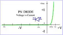
Forward-biased diodes have low impedance approximating a short circuit with a small voltage drop, while reverse-biased diodes have a very high impedance approximating an open circuit. The diode symbol's arrow shows the forward-biased direction of conventional current flow.
Diode AND and OR logic gates
Each input of a diode logic gate connects through a diode connected to a shared wired logic output. Depending on the voltage level of each input and direction of the diode, each diode may or may not be forward-biased. If any are forward-biased, the shared output wire will be one small forward voltage drop within the forward-biased diode's input.
If no diode is forward-biased then no diode will provide drive current for the output's load (such as a subsequent logic stage). So the output additionally requires a pull-up or pull-down resistor connected to a voltage source, so that the output can transition quickly[lower-alpha 1] and provide a strong driving current when no diodes are forward-biased.
Note: the following circuits have two inputs for each gate and thus use two diodes, but can be extended with more diodes to allow for more inputs. At least one input of every gate must be connected to a strong-enough high or low voltage source. If all inputs are disconnected from a strong source, the output may not fall within a valid voltage range.
Active-high OR logic gate
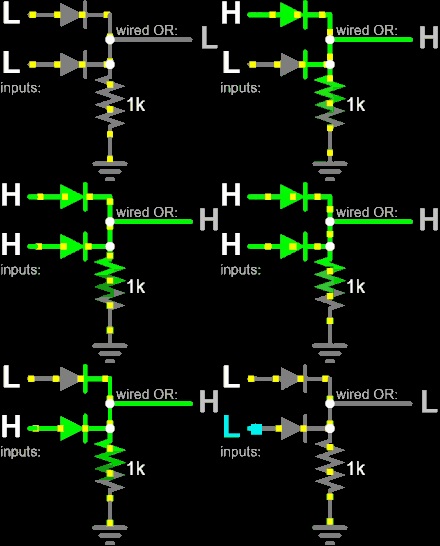
Each input connects to the anode of a diode. All cathodes are connected to the output, which has a pull-down resistor.
If any input is high, its diode will be forward-biased and conduct current, and thus pull the output voltage high[lower-alpha 2].
If all inputs are low, all diodes will be reverse-biased and so none will conduct current. The pull-down resistor will quickly pull the output voltage low.
In summary, if any input is high the output will be high, but only if all inputs are low will the output be low:
| inputs | output | |
|---|---|---|
| Low | Low | Low |
| Low | High | High |
| High | Low | High |
| High | High | High |
This corresponds to logical OR in active-high logic, as well as simultaneously to logical AND in active-low logic.
Active-high AND logic gate
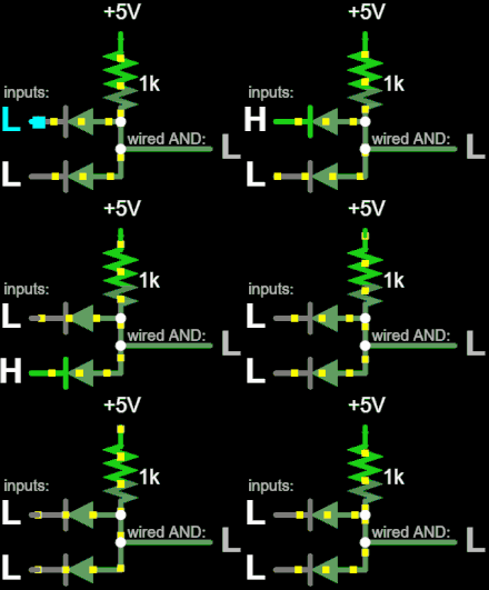
This circuit mirrors the previous gate: the diodes are reversed so that each input connects to the cathode of a diode and all anodes are connected together to the output, which has a pull-up resistor.
If any input is low, its diode will be forward-biased and will conduct current, and thus pull the output voltage low[lower-alpha 3].
If all inputs are high, all diodes will be reverse-biased and so none will conduct current. The pull-up resistor will quickly pull the output voltage high.
In summary, if any input is low, the output will be low, but only if all inputs are high will the output be high:
| inputs | output | |
|---|---|---|
| Low | Low | Low |
| Low | High | Low |
| High | Low | Low |
| High | High | High |
This corresponds to logical AND in active-high logic, as well as simultaneously to logical OR in active-low logic.
Real diode considerations
For simplicity, diodes may sometimes be assumed to have no voltage drop or resistance when forward-biased and infinite resistance when reverse-biased. But real diodes are better approximated by the Shockley diode equation, which has an more complicated exponential current–voltage relationship called the diode law.
Designers must rely on a diode's specification sheet, which primarily provides a maximum forward voltage drop at one or more forward currents, a reverse leakage current (or saturation current), and a maximum reverse voltage limited by Zener or avalanche breakdown. Effects of temperature and process variation are usually included. Typical examples:
- Germanium diode:
- Max forward voltage at 10 mA = 1 volt @ 0 to 85 °C[lower-alpha 4]
- Max reverse leakage current at 15 volts = 100 microamps @ 85 °C
- Silicon diode:
- Max forward voltage at 10 mA = 1 volt @ 0 to 125 °C
- Max reverse leakage current at 15 volts = 1 microamp @ 85 °C[lower-alpha 5]
Transient response
Diodes also have a transient response that might be of concern. The capacitance between anode and cathode is inversely proportional to the reverse voltage, growing as it approaches 0 volts and into forward bias.
There is also a recovery concern: a diode's current will not decrease immediately when switching from forward-biased to reverse-biased, because discharging its stored charge takes a finite amount of time (trr or reverse recovery time).[1] In a diode OR gate, if two or more of the inputs are high and one switches to low, recovery issues will cause a short-term dip in the output voltage or increase current in the diodes that remain high. If a diode–transistor logic gate drives a transistor inverter of similar construction, the transistor will have a similar base-collector capacitance that is amplified by the transistor gain, so that it will be too slow to pass the glitch. But when the diode is much slower, recovery will become a concern:
In one unusual design, small selenium diode discs were used with germanium transistors. The recovery time of the very slow selenium diodes caused a glitch on the inverter output. It was fixed by placing a selenium diode across the base-emitter junction of the transistor making it think it was a selenium transistor (if there could ever be one).
Voltage losses
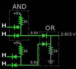
Active logic gates output voltages within a precise voltage range, provided that their input voltages were within a somewhat wider valid input voltage range. This level restoration allows more cascaded logic stages and removes noise, facilitating very large scale integration.
However, passive diode logic gates accumulate the following voltage losses when gates are cascaded:
- Forward voltage VF drop
- High voltages inputted to every OR gate are reduced by VF (~0.6 V in silicon, ~0.3 V in germanium), while low voltages inputted to every AND gate are raised by VF.
- Source resistance
- A voltage source's output resistance and the subsequent gate's pull-up/down resistor form a voltage divider that weakens voltage levels. This decreases high voltages in OR gates and increases low voltages in AND gates.
Thus the feasible amount of cascading is limited by the value of VF and the high-low voltage difference. With special designs, two-stage systems are sometimes achieved.
In order to compensate for the voltage drop and provide sufficient current to drive the next circuit(s) load, the pull-up resistors may be connected to a supply higher than the nominal high voltage level and similarly the pull-down resistors may be connected to a supply lower than the nominal low voltage.
Applications
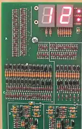
Historically, diode logic was used extensively in the construction of early computers, since semiconductor diodes could replace bulky and costly active vacuum tubes. The invention of the transistor allowed transistors to replace tubes as the active element in diode–transistor logic. Since early transistors were not reliable, the D-17B missile guidance computer, for instance, primarily used diode logic and only used transistors when necessary. Transistors quickly advanced to replace diode logic almost entirely. However, diode logic still finds some modern uses.
Cheap passive logic from active outputs
Low-impedance push–pull outputs of conventional ICs shouldn't directly be connected to external circuitry, as they may create a short circuit between power and ground. Such outputs, however, may be used as inputs to passive AND or OR diode logic gates. This avoids the costs of adding active logic gates.[3] However, diode logic will degrade voltage levels and result in poor noise rejection, so designers should be aware of the interfaced logic family's voltage ranges and limitations, to prevent failures.
Mickey Mouse Logic
The humorously-named "Micky Mouse Logic" described in Don Lancaster's CMOS Cookbook suggests using diodes as a multi-tool for augmenting the limited capabilities of regular CMOS 4000-series ICs, for instance by using a diode OR gate to add extra inputs on a flip-flop, or a diode AND gate to configure a divide-by-N counter.[4] A variant approach suggests keeping a supply of 1N914 diodes with inverting Schmitt trigger ICs to provide hysteresis and functional completeness.[5]
Any key interrupt
An active-low OR diode logic gate is formed by a keypad containing diodes at each switch, all connected to a shared pull-up resistor. When no switch is closed, the pull-up keeps the output high. But when the switch for any key connects to ground, the output goes low. This OR result can be used as an interrupt signal to indicate that any key has been pressed. Then a microcontroller can wake from power-saving standby and scan the key matrix to determine which key specifically was pressed.[6]
Tunnel diodes
During the 1960s the use of tunnel diodes in logic circuits was an active research topic. When compared to transistor logic gates of the time, the tunnel diode offered much higher speeds. Unlike other diode types, the tunnel diode offered the possibility of amplification of signals at each stage. The operating principles of a tunnel diode logic rely on biasing of the tunnel diode and supply of current from inputs over a threshold current, to switch the diode between two states. Consequently, tunnel diode logic circuits required a means to reset the diode after each logical operation.
However, a simple tunnel diode gate offered little isolation between inputs and outputs and had low fan in and fan out. More complex gates, with additional tunnel diodes and bias power supplies, overcame some of these limitations.[7] Advances in discrete and integrated circuit transistor speed and the more nearly unilateral nature of transistor amplifiers overtook the tunnel diode gate, resulting in it no longer being used in modern computers.
Notes
- The output load will have some capacitance (even if no capacitor is added, there will be some parasitic capacitance). When all diodes are reversed biased in a high impedance state, they will only provide a minuscule amount of reverse saturation current for draining the capacitance, thus it will take too long for the output voltage to fully transition. Diodes also have a reverse recovery time.
- The output will be pulled specifically to one forward voltage drop less than the lowest high input voltage. The designer must ensure this output voltage should still lie within the valid high range.
- The output will be pulled specifically to one forward voltage drop above the highest low input voltage. The designer must ensure this output voltage should still lie within the valid low range.
- More realistically the germanium forward voltage might be 0.25 to 0.4 volts but this is often not specified.
- The silicon leakage current might be much lower, possibly 1 to 100 nanoamps.
References
- "Reverse Recovery Time". Analog Devices. Archived from the original on 2023-01-18. Retrieved 2023-01-18.
- Bigelow, Ken (2015), Diode logic, archived from the original 7 May 2021.
- Integrated Circuits §Using diodes to combine outputs, Electronics Club, retrieved 27 November 2022.
- Lancaster, Don (1977). CMOS Cookbook (2nd ed.). USA: Howard W Sams & Co. pp. 242–245. ISBN 0 672-22459-3.
- Wilson, Ray. "CMOS Mickey Mouse Logic". musicfromouterspace.com. Archived from the original on 2022-09-16. Retrieved 2023-01-18.
- section 46.3.5 "Keypad Standby" on pg 2884 of "i.MX RT1060X Processor Reference Manual", Rev. 1, 05/2022
- Tunnel Diodes for Switching and Microwave Applications Technical Manual TD-30, RCA 1963, (3rd Chapter) Switching
