Indium gallium arsenide
Indium gallium arsenide (InGaAs) (alternatively gallium indium arsenide, GaInAs) is a ternary alloy (chemical compound) of indium arsenide (InAs) and gallium arsenide (GaAs). Indium and gallium are group III elements of the periodic table while arsenic is a group V element. Alloys made of these chemical groups are referred to as "III-V" compounds. InGaAs has properties intermediate between those of GaAs and InAs. InGaAs is a room-temperature semiconductor with applications in electronics and photonics.
The principal importance of GaInAs is its application as a high-speed, high sensitivity photodetector of choice for optical fiber telecommunications.[1]
Nomenclature
Indium gallium arsenide (InGaAs) and gallium-indium arsenide (GaInAs) are used interchangeably. According to IUPAC standards[2] the preferred nomenclature for the alloy is GaxIn1-xAs where the group-III elements appear in order of increasing atomic number, as in the related alloy system AlxGa1-xAs. By far, the most important alloy composition from technological and commercial standpoints is Ga0.47In0.53As, which can be deposited in single crystal form on indium phosphide (InP).
Materials synthesis
GaInAs is not a naturally-occurring material. Single crystal material is required for electronic and photonic device applications. Pearsall and co-workers were the first to describe single-crystal epitaxial growth of In0.53Ga0.47As on (111)-oriented [3] and on (100)-oriented [4] InP substrates. Single crystal material in thin-film form can be grown by epitaxy from the liquid-phase (LPE), vapour-phase (VPE), by molecular beam epitaxy (MBE), and by metalorganic chemical vapour deposition (MO-CVD).[5] Today, most commercial devices are produced by MO-CVD or by MBE.
The optical and mechanical properties of InGaAs can be varied by changing the ratio of InAs and GaAs, In
1-xGa
xAs.[6] Most InGaAs devices are grown on indium phosphide (InP) substrates. In order to match the lattice constant of InP and avoid mechanical strain, In
0.53Ga
0.47As is used. This composition has an optical absorption edge at 0.75 eV, corresponding to a cut-off wavelength of λ=1.68 μm at 295 K.
By increasing the mole fraction of InAs further compared to GaAs, it is possible to extend the cut-off wavelength up to about λ=2.6 μm. In that case special measures have to be taken to avoid mechanical strain from differences in lattice constants.
GaAs is lattice-mismatched to germanium (Ge) by 0.08%. With the addition of 1.5% InAs to the alloy, In0.015Ga0.985As becomes latticed-matched to the Ge substrate, reducing stress in subsequent deposition of GaAs.
Electronic and optical properties
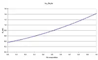
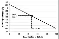
InGaAs has a lattice parameter that increases linearly with the concentration of InAs in the alloy.[7] The liquid-solid phase diagram[3] shows that during solidification from a solution containing GaAs and InAs, GaAs is taken up at a much higher rate than InAs, depleting the solution of GaAs. During growth from solution, the composition of first material to solidify is rich in GaAs while the last material to solidify is richer in InAs. This feature has been exploited to produce ingots of InGaAs with graded composition along the length of the ingot. However, the strain introduced by the changing lattice constant causes the ingot to be polycrystalline and limits the characterization to a few parameters, such as bandgap and lattice constant with uncertainty due to the continuous compositional grading in these samples.
Properties of single crystal GaInAs
Single crystal GaInAs
Single crystal epitaxial films of GaInAs can be deposited on a single crystal substrate of III-V semiconductor having a lattice parameter close to that of the specific gallium indium arsenide alloy to be synthesized. Three substrates can be used: GaAs, InAs and InP. A good match between the lattice constants of the film and substrate is required to maintain single crystal properties and this limitation permits small variations in composition on the order of a few percent. Therefore, the properties of epitaxial films of GaInAs alloys grown on GaAs are very similar to GaAs and those grown on InAs are very similar to InAs, because lattice mismatch strain does not generally permit significant deviation of the composition from the pure binary substrate.
Ga
0.47In
0.53As is the alloy whose lattice parameter matches that of InP at 295 K. GaInAs lattice-matched to InP is a semiconductor with properties quite different from GaAs, InAs or InP. It has an energy band gap of 0.75 eV, an electron effective mass of 0.041 and an electron mobility close to 10,000 cm2·V−1·s−1 at room temperature, all of which are more favorable for many electronic and photonic device applications when compared to GaAs, InP or even Si.[1] Measurements of the band gap and electron mobility of single-crystal GaInAs were first published by Takeda and co-workers.[9]
| Property | Value at 295 K | Reference |
|---|---|---|
| Lattice Parameter | 5.869 Å | [4] |
| Band Gap | 0.75 eV | [9] |
| Electron effective mass | 0.041 | [10] |
| Light-hole effective mass | 0.051 | [11] |
| Electron mobility | 10,000 cm2·V−1·s−1 | [12] |
| Hole mobility | 250 cm2·V−1·s−1 | [12] |
FCC lattice parameter
Like most materials, the lattice parameter of GaInAs is a function of temperature. The measured coefficient of thermal expansion [13] is 5.66×10⁻⁶ K−1. This is significantly larger than the coefficient for InP which is 4.56×10⁻⁶ K−1. A film that is exactly lattice-matched to InP at room temperature is typically grown at 650 °C with a lattice mismatch of +6.5×10⁻⁴. Such a film has a mole fraction of GaAs = 0.47. To obtain lattice matching at the growth temperature, it is necessary to increase the GaAs mole fraction to 0.48.
Bandgap energy
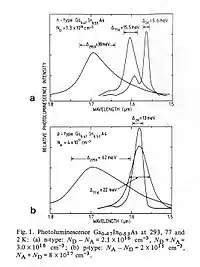
The bandgap energy of GaInAs can be determined from the peak in the photoluminescence spectrum, provided that the total impurity and defect concentration is less than 5×1016 cm−3. The bandgap energy depends on temperature and increases as the temperature decreases, as can be seen in Fig. 3 for both n-type and p-type samples. The bandgap energy at room temperature for standard InGaAs/InP (53% InAs, 47% GaAs), is 0.75 eV and lies between that of Ge and Si. By coincidence the bandgap of GaInAs is perfectly placed for photodetector and laser applications for the long-wavelength transmission window, (the C-band and L-band) for fiber-optic communications.
Effective mass
The electron effective mass of GaInAs m*/m° = 0.041 [10] is the smallest for any semiconductor material with an energy bandgap greater than 0.5 eV. The effective mass is determined from the curvature of the energy-momentum relationship: stronger curvature translates into lower effective mass and a larger radius of delocalization. In practical terms, a low effective mass leads directly to high carrier mobility, favoring higher speed of transport and current carrying capacity. A lower carrier effective mass also favors increased tunneling current, a direct result of delocalization.
The valence band has two types of charge carriers: light holes: m*/m° = 0.051 [11] and heavy holes: m*/m° = 0.2.[14] The electrical and optical properties of the valence band are dominated by the heavy holes, because the density of these states is much greater than that for light holes. This is also reflected in the mobility of holes at 295 K, which is a factor of 40 lower than that for electrons.
Mobility of electrons and holes
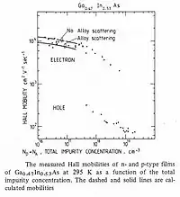
Electron mobility and hole mobility are key parameters for design and performance of electronic devices. Takeda and co-workers were the first to measure electron mobility in epitaxial films of InGaAs on InP substrates.[9] Measured carrier mobilities for electrons and holes are shown in Figure 4.
The mobility of carriers in Ga
0.47In
0.53As is unusual in two regards:
- The very high value of electron mobility
- The unusually large ratio of electron to hole mobility.
The room temperature electron mobility for reasonably pure samples of Ga
0.47In
0.53As approaches 10×103 cm2·V−1·s−1, which is the largest of any technologically important semiconductor, although significantly less than that for graphene.
The mobility is proportional to the carrier conductivity. As mobility increases, so does the current-carrying capacity of transistors. A higher mobility shortens the response time of photodetectors. A larger mobility reduces series resistance, and this improves device efficiency and reduces noise and power consumption.
The minority carrier diffusion constant is directly proportional to carrier mobility. The room temperature diffusion constant for electrons at 250 cm2·s−1 is significantly larger than that of Si, GaAs, Ge or InP, and determines the ultra-fast response of Ga
0.47In
0.53As photodetectors.
The ratio of electron to hole mobility is the largest of currently-used semiconductors.
Applications
Photodetectors
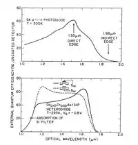
The principal application of GaInAs is as an infrared detector. The spectral response of a GaInAs photodiode is shown in Figure 5. GaInAs photodiodes are the preferred choice in the wavelength range of 1.1 μm < λ < 1.7 μm. For example, compared to photodiodes made from Ge, GaInAs photodiodes have faster time response, higher quantum efficiency and lower dark current for the same sensor area.[16] GaInAs photodiodes were invented in 1977 by Pearsall.[17]
Avalanche photodiodes offer the advantage of additional gain at the expense of response time. These devices are especially useful for detection of single photons in applications such as quantum key distribution where response time is not critical. Avalanche photodetectors require a special structure to reduce reverse leakage current due to tunnelling. The first practical avalanche photodiodes were designed and demonstrated in 1979.[18]
In 1980, Pearsall developed a photodiode design that exploits the uniquely short diffusion time of high mobility of electrons in GaInAs, leading to an ultrafast response time.[19][20] This structure was further developed and subsequently named the UTC, or uni-travelling carrier photodiode.[21] In 1989, Wey and co-workers[22] designed and demonstrated a p-i-n GaInAs/InP photodiodes with a response time shorter than 5 picoseconds for a detector surface measuring 5 μm x 5 μm.
Other important innovations include the integrated photodiode – FET receiver[23] and the engineering of GaInAs focal-plane arrays.[24]
Lasers
Semiconductor lasers are an important application for GaInAs, following photodetectors. GaInAs can be used as a laser medium. Devices have been constructed that operate at wavelengths of 905 nm, 980 nm, 1060 nm, and 1300 nm. InGaAs quantum dots on GaAs have also been studied as lasers.[25] GaInAs/InAlAs quantum-well lasers can be tuned to operate at the λ = 1500 nm low-loss, low-dispersion window for optical fiber telecommunications [26] In 1994, GaInAs/AlInAs quantum wells were used by Jérôme Faist and co-workers[27] who invented and demonstrated a new kind of semiconductor laser based on photon emission by an electron making an optical transition between subbands in the quantum well. They showed that the photon emission regions can be cascaded in series, creating the quantum cascade laser (QCL). The energy of photon emission is a fraction of the bandgap energy. For example, GaInAs/AlInAs QCL operates at room temperature in the wavelength range 3 μm < λ < 8 μm. The wavelength can be changed by modifying the width of the GaInAs quantum well.[28] These lasers are widely used for chemical sensing and pollution control.
Photovoltaics and transistors
GaInAs is used in triple-junction photovoltaics and also for thermophotovoltaic power generation.[29]
In
0.015Ga
0.985As can be used as an intermediate band-gap junction in multi-junction photovoltaic cells with a perfect lattice match to Ge. The perfect lattice match to Ge reduces defect density, improving cell efficiency.
HEMT devices using InGaAs channels are one of the fastest types of transistor[30]
In 2012 MIT researchers announced the smallest transistor ever built from a material other than silicon.[31] The Metal oxide semiconductor field-effect transistor (MOSFET) is 22 nanometers long. This is a promising accomplishment, but more work is needed to show that the reduced size results in improved electronic performance relative to that of silicon or GaAs-based transistors.
In 2014, Researchers at Penn State University developed a novel device prototype designed to test nanowires made of compound semiconductors such as InGaAs.[32] The goal of this device was to see if a compound material would retain its superior mobility at nanoscale dimensions in a FinFET device configuration. The results of this test sparked more research, by the same research team, into transistors made of InGaAs which showed that in terms of on current at lower supply voltage, InGaAs performed very well compared to existing silicon devices.
In Feb 2015 Intel indicated it may use InGaAs for its 7 nanometer CMOS process in 2017.[33]
Safety and toxicity
The synthesis of GaInAs, like that of GaAs, most often involves the use of arsine (AsH
3), an extremely toxic gas. Synthesis of InP likewise most often involves phosphine (PH
3). Inhalation of these gases neutralizes oxygen absorption by the bloodstream and can be fatal within a few minutes if toxic dose levels are exceeded. Safe handling involves using a sensitive toxic gas detection system and self-contained breathing apparatus.[34]
Once GaInAs is deposited as a thin film on a substrate, it is basically inert and is resistant to abrasion, sublimation or dissolution by common solvents such as water, alcohols or acetones. In device form the volume of the GaInAs is usually less than 1000 μm3, and can be neglected compared to the volume of the supporting substrate, InP or GaAs.
The National Institutes of Health studied these materials and found:[35]
- No evidence of carcinogenic activity of gallium arsenide in male F344/N rats exposed to 0.01, 0.1, or 1.0 mg/m3
- Carcinogenic activity in female F344/N rats
- No evidence of carcinogenic activity in male or female B6C3F1 mice exposed to 0.1, 0.5, or 1.0 mg/m3.
The World Health Organization's International Agency for Research on Cancer's review of the NIH toxicology study concluded:[36]
- There is inadequate evidence in humans for the carcinogenicity of gallium arsenide.
- There is limited evidence in experimental animals for the carcinogenicity of gallium arsenide.
- The gallium moiety may be responsible for lung cancers observed in female rats
REACH (Registration, Evaluation, Authorisation and Restriction of Chemicals) is a European initiative to classify and regulate materials that are used, or produced (even as waste) in manufacturing. REACH considers three toxic classes: carcinogenic, reproductive, and mutagenic capacities.
The REACH classification procedure consists of two basic phases. In phase one the hazards intrinsic to the material are determined, without any consideration of how the material might be used or encountered in the work place or by a consumer. In phase two the risk of harmful exposure is considered along with procedures that can mitigate exposure. Both GaAs and InP are in phase 1 evaluation. The principal exposure risk occurs during substrate preparation where grinding and polishing generate micron-size particles of GaAs and InP. Similar concerns apply to wafer dicing to make individual devices. This particle dust can be absorbed by breathing or ingestion. The increased ratio of surface area to volume for such particles increases their chemical reactivity.
Toxicology studies are based on rat and mice experiments. No comparable studies test the effects of ingesting GaAs or InP dust in a liquid slurry.
The REACH procedure, acting under the precautionary principle, interprets "inadequate evidence for carcenogenicity" as "possible carcinogen". As a result, the European Chemicals Agency classified InP in 2010 as a carcinogen and reproductive toxin:[37]
- Classification & labelling in accordance with Directive 67/548/EEC
- Classification: Carc. Cat. 2; R45
- Repr. Cat. 3; R62
and ECHA classified GaAs in 2010 as a carcinogen and reproductive toxin:
- Classification & labelling in accordance with Directive 67/548/EEC:
- Classification3: Carc. Cat. 1; R45
- Repro. Cat. 2; R60
References
- Pearsall, T. (1980). "Ga0.47In0.53As: A ternary semiconductor for photodetector applications". IEEE Journal of Quantum Electronics. Institute of Electrical and Electronics Engineers (IEEE). 16 (7): 709–720. doi:10.1109/jqe.1980.1070557. ISSN 0018-9197.
- "International Union of Pure and Applied Chemistry: Home". IUPAC. Retrieved 2013-09-22.
- Pearsall, T. P.; Hopson, R. W. (1977). "Growth and characterization of lattice‐matched epitaxial films of GaxIn1−xAs/InP by liquid‐phase epitaxy". Journal of Applied Physics. AIP Publishing. 48 (10): 4407–4409. doi:10.1063/1.323399. ISSN 0021-8979.
- Pearsall, T. P.; Bisaro, R.; Ansel, R.; Merenda, P. (1978-04-15). "The growth of GaxIn1−xAs on (100) InP by liquid‐phase epitaxy". Applied Physics Letters. AIP Publishing. 32 (8): 497–499. doi:10.1063/1.90100. ISSN 0003-6951.
- Hirtz, J.P.; Larivain, J.P.; Duchemin, J.P.; Pearsall, T.P.; Bonnet, M. (1980). "Growth of Ga0.47In0.53As on InP by low-pressure m.o. c.v.d.". Electronics Letters. Institution of Engineering and Technology (IET). 16 (11): 415–416. doi:10.1049/el:19800290. ISSN 0013-5194.
- "Technology: What is InGaAs?". Sensorsinc.com. Archived from the original on 2013-10-29. Retrieved 2013-12-02.
- John W. Wagner. "Preparation and Properties of Bulk In1 − x Ga x As Alloys : SOLID STATE SCIENCE - Technical Papers". Jes.ecsdl.org. Retrieved 2013-12-02.
- Pearsall, T. P.; Eaves, L.; Portal, J. C. (1983). "Photoluminescence and impurity concentration in GaxIn1−xAsyP1−y alloys lattice-matched to InP". Journal of Applied Physics. 54 (2): 1037. Bibcode:1983JAP....54.1037P. doi:10.1063/1.332122.
- Y. Takeda, A. Sasaki, Y. Imamura, and T. Takagi, "Electron mobility and energy gap of In
0.53Ga
0.47As on InP substrate", J. of Appl. Physics 47, 5405-7 (1976); https://doi.org/10.1063/1.322570 - Nicholas, R. J.; Portal, J. C.; Houlbert, C.; Perrier, P.; Pearsall, T. P. (1979-04-15). "An experimental determination of the effective masses for GaxIn1−xAsyP1−y alloys grown on InP". Applied Physics Letters. AIP Publishing. 34 (8): 492–494. doi:10.1063/1.90860. ISSN 0003-6951.
- Hermann, Claudine; Pearsall, Thomas P. (1981-03-15). "Optical pumping and the valence‐band light‐hole effective mass in GaxIn1−xAsyP1−y (y≃2.2x)". Applied Physics Letters. AIP Publishing. 38 (6): 450–452. doi:10.1063/1.92393. ISSN 0003-6951.
- Pearsall, T.P.; Hirtz, J.P. (1981). "The carrier mobilities in Ga0.47In0.53 as grown by organo-mettalic [sic] CVD and liquid-phase epitaxy". Journal of Crystal Growth. Elsevier BV. 54 (1): 127–131. doi:10.1016/0022-0248(81)90258-x. ISSN 0022-0248.
- Bisaro, R.; Merenda, P.; Pearsall, T. P. (1979). "The thermal‐expansion parameters of some GaxIn1−xAsyP1−x alloys". Applied Physics Letters. AIP Publishing. 34 (1): 100–102. doi:10.1063/1.90575. ISSN 0003-6951.
- Lin, S. Y. (1989). "Cyclotron resonance of two-dimensional holes in strained-layer quantum well structure of (100)In0.20Ga0.80As/GaAs". Applied Physics Letters. 55 (7): 666–668. Bibcode:1989ApPhL..55..666L. doi:10.1063/1.101816.
- T.P. Pearsall, "InGaAs Photodetectors" in Properties of Lattice-Matched and Strained Indium Gallium Arsenide, ed P.Bhattacharya, (London, IEE Press, 1993) pp267-77.
- Pearsall, T.P.; Pollack, M.A. (3 June 1985). Tsang, W. T. (ed.). Photodiodes for Optical Fiber Communication. pp. 174–246. ISBN 978-0-08-086417-4.
{{cite book}}:|work=ignored (help) - T.P. Pearsall and R.W. Hopson, Jr, Electronic Materials Conference, Cornell University, 1977, published in J. Electron. Mat. 7, pp.133-146, (1978)
- Nishida, Katsuhiko (1979). "InGaAsP heterostructure avalanche photodiodes with high avalanche gain". Applied Physics Letters. 35 (3): 251–253. Bibcode:1979ApPhL..35..251N. doi:10.1063/1.91089.
- Pearsall, T. (1981). "A Ga0.47In0.53As/InP heterophotodiode with reduced dark current". IEEE Journal of Quantum Electronics. 17 (2): 255–259. Bibcode:1981IJQE...17..255P. doi:10.1109/JQE.1981.1071057.
- Pearsall, T.P.; Logan, R.A.; Bethea, C.G. (1983). "GaInAs/InP large bandwidth (> 2 GHz) PIN detectors". Electronics Letters. Institution of Engineering and Technology (IET). 19 (16): 611–612. doi:10.1049/el:19830416. ISSN 0013-5194.
- Shimizu, N. (1998). "InP-InGaAs uni-traveling-carrier photodiode with improved 3-dB bandwidth of over 150 GHz". IEEE Photonics Technology Letters. 10 (3): 412–414. Bibcode:1998IPTL...10..412S. doi:10.1109/68.661427.
- Wey, Y. G.; Crawford, D. L.; Giboney, K.; Bowers, J. E.; Rodwell, M. J.; Silvestre, P.; Hafich, M. J.; Robinson, G. Y. (1991-05-13). "Ultrafast graded double‐heterostructure GaInAs/InP photodiode". Applied Physics Letters. AIP Publishing. 58 (19): 2156–2158. doi:10.1063/1.104991. ISSN 0003-6951.
- Veteran, J.L. (1982). "Schottky barrier measurements on p-type In0.53Ga0.47As". Thin Solid Films. 97 (2): 187–190. Bibcode:1982TSF....97..187V. doi:10.1016/0040-6090(82)90227-9.
- "Sensors Unlimited - InGaAs Near and Short Wave Infrared (SWIR) Cameras, Arrays, and Photodiodes". Sensorsinc.com. Retrieved 2013-09-22.
- Bimberg, D.; Kirstaedter, N.; Ledentsov, N.N.; Alferov, Zh.I.; Kop'ev, P.S.; Ustinov, V.M. (1997). "InGaAs-GaAs quantum-dot lasers". IEEE Journal of Selected Topics in Quantum Electronics. Institute of Electrical and Electronics Engineers (IEEE). 3 (2): 196–205. doi:10.1109/2944.605656. ISSN 1077-260X.
- K. Alavi, H. Temkin, A.Y. Cho, and T.P. Pearsall, "AlInAs-GaInAs Multi Quantum-Well Lasers Emitting at 1.55μm", Appl. Phys. Lett. 4244, 845-847 (1983)
- Faist, J.; Capasso, F.; Sivco, D. L.; Sirtori, C.; Hutchinson, A. L.; Cho, A. Y. (1994-04-22). "Quantum Cascade Laser". Science. American Association for the Advancement of Science (AAAS). 264 (5158): 553–556. doi:10.1126/science.264.5158.553. ISSN 0036-8075. PMID 17732739.
- J. Faist, Quantum Cascade Laser, (Oxford, Oxford University Press, 2013)
- M.Tan, L.Ji, Y.Wu, P.Dai, Q.Wang, K.Li, T.Yu, Y.Yu, S.Lu and H.Yang, "Investigation of InGaAs thermophotovoltaic cells under blackbody radiation", Applied Physics Express 7,p. 096601 (2014), https://doi.org/10.7567/APEX.7.096601
- Archived January 4, 2006, at the Wayback Machine
- "Tiny compound semiconductor transistor could challenge silicon's dominance".
- Thathachary, Arun V.; Agrawal, Nidhi; Liu, Lu; Datta, Suman (January 1, 2014). "Electron Transport in Multigate InxGa1–x As Nanowire FETs: From Diffusive to Ballistic Regimes at Room Temperature". Nano Letters. 14 (2): 626–633. Bibcode:2014NanoL..14..626T. doi:10.1021/nl4038399. PMID 24382089.
- Sebastian Anthony (23 Feb 2015). "Intel forges ahead to 10nm, will move away from silicon at 7nm". Ars Technica. Retrieved 28 Nov 2019.
- The environment, health and safety aspects of indium gallium arsenide sources (such as trimethylgallium, trimethylindium and arsine) and industrial hygiene monitoring studies of standard MOVPE have been reviewed. Shenai-Khatkhate, D.V.; et al. (2004). "Environment, health and safety issues for sources used in MOVPE growth of compound semiconductors". Journal of Crystal Growth. 272 (1–4): 816–821. Bibcode:2004JCrGr.272..816S. doi:10.1016/j.jcrysgro.2004.09.007.
- "NTP Technical Report on the Toxicology and Carcinogenesis Studies of Gallium Arsenide" (PDF). Ntp.niehs.nih.gov. Retrieved 2013-09-22.
- "IARC Monographs on the Evaluation of Carcinogenic Risks to Humans" (PDF). Monographs.iarc.fr. Retrieved 2013-09-22.
- "Homepage - ECHA". Echa.europa.eu. Retrieved 2013-09-22.
External links
- NSM data archive at the Ioffe Institute, St. Petersburg, Russia