Gold plating
Gold plating is a method of depositing a thin layer of gold onto the surface of another metal, most often copper or silver (to make silver-gilt), by chemical or electrochemical plating. This article covers plating methods used in the modern electronics industry; for more traditional methods, often used for much larger objects, see gilding.


Types
There are several types of gold plating used in the electronics industry:[1]
- Soft, pure gold plating is used in the semiconductor industry. The gold layer is easily soldered and wire bonded. Its Knoop hardness ranges between 60 and 85. The plating baths have to be kept free of contamination.
- Soft, pure gold is deposited from special electrolytes. Entire printed circuit boards can be plated. This technology can be used for depositing layers suitable for wire bonding.
- Bright hard gold on contacts, with Knoop hardness between 120–300 and purity of 99.7–99.9% gold. Often contains a small amount of nickel and/or cobalt; these elements interfere with die bonding, therefore the plating baths cannot be used for semiconductors.
- Bright hard gold on printed circuit board tabs is deposited using lower concentration of gold in the baths. Usually contains nickel and/or cobalt as well. Edge connectors are often made by controlled-depth immersion of only the edge of the boards.
Gold plating chemistry
There are five recognized classes of gold plating chemistry:
- Alkaline gold cyanide, for gold and gold alloy plating
- Neutral gold cyanide, for high-purity plating
- Acid gold plating for bright hard gold and gold alloy plating
- Non-cyanide, generally sulphite or chloride-based for gold and gold alloy plating
- Miscellaneous
Jewelry
Gold plating of silver is used in the manufacture of jewelry. The thickness of gold plating on jewellery is noted in microns (or micro-meters). The microns of thickness determines how long the gold plating lasts with usage. The jewellery industry denotes different qualities of gold plating in the following terminology
- Gold flashed / Gold washed - gold layer thickness less than 0.5 micron
- Gold plated - gold layer thickness greater than or equal to 0.5 micron
- Heavy gold plated / Vermeil - gold layer thickness greater than or equal to 2.5 micron
Gold plated silver jewellery can still tarnish as the silver atoms diffuse into the gold layer, causing slow gradual fading of its color and eventually causing tarnishing of the surface. This process may take months and even years, depending on the thickness of the gold layer. A barrier metal layer is used to counter this effect - these can be nickel or rhodium. Copper, which also migrates into gold, does so more slowly than silver. The copper is usually further plated with nickel. A gold-plated silver article is usually a silver substrate with layers of copper, nickel, and gold deposited on top of it.
Infrared reflectivity
Gold, applied by evaporated methods or electroplating, has been specified by NASA to thermally control spacecraft instruments, due to its 99% reflectivity in infrared wavelengths.
Electronics

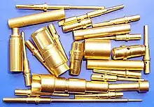
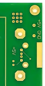
Gold plating is often used in electronics, to provide a corrosion-resistant electrically conductive layer on copper, typically in electrical connectors and printed circuit boards.
With direct gold-on-copper plating, the copper atoms tend to diffuse through the gold layer, causing tarnishing of its surface and formation of an oxide and/or sulphide layer.
A layer of a suitable barrier metal, usually nickel, is often deposited on the copper substrate before the gold plating. The layer of nickel provides mechanical backing for the gold layer, improving its wear resistance. It also reduces the impact of pores present in the gold layer.
Both the nickel and gold layers can be plated by electrolytic or electroless processes. There are many factors to consider in selection of either electrolytic or electroless plating methods. These include what the deposit will be used for, configuration of the part, materials compatibility and cost of processing. In different applications, electrolytic or electroless plating can have cost advantages.
At higher frequencies, the skin effect may cause higher losses due to higher electrical resistance of nickel; a nickel-plated trace can have its useful length shortened three times in the 1 GHz band in comparison with the non-plated one. Selective plating is used, depositing the nickel and gold layers only on areas where it is required and does not cause the detrimental side effects.[2]
Gold plating may lead to formation of gold whiskers.
Wire bonding between gold plated contacts and aluminium wires or between aluminium contacts and gold wires under certain conditions develops a brittle layer of gold-aluminium intermetallics, known as purple plague.
Soldering issues

Soldering gold-plated parts can be problematic as gold is soluble in solder. Solder which contains more than 4–5% gold can become brittle. The joint surface is dull-looking.
Gold reacts with both tin and lead in their liquid state, forming brittle intermetallics. When eutectic 63% tin – 37% lead solder is used, no lead-gold compounds are formed, because gold preferentially reacts with tin, forming the AuSn
4 compound. Particles of AuSn
4 disperse in the solder matrix, forming preferential cleavage planes, significantly lowering the mechanical strength and therefore reliability of the resulting solder joints.
If the gold layer does not completely dissolve into the solder, then slow intermetallic reactions can proceed in the solid state as the tin and gold atoms cross-migrate. Intermetallics have poor electrical conductivity and low strength. The ongoing intermetallic reactions also cause Kirkendall effect, leading to mechanical failure of the joint, similar to the degradation of gold-aluminium bonds known as purple plague.
A 2–3 µm layer of gold dissolves completely within one second during typical wave soldering conditions. Layers of gold thinner than 0.5 µm (0.02 thou) also dissolve completely into the solder, exposing the underlying metal (usually nickel) to the solder. Impurities in the nickel layer can prevent the solder from bonding to it. Electroless nickel plating contains phosphorus. Nickel with more than 8% phosphorus is not solderable. Electrodeposited nickel may contain nickel hydroxide. An acid bath is required to remove the passivation layer before applying the gold layer; improper cleaning leads to a nickel surface difficult to solder. A stronger flux can help, as it aids dissolving the oxide deposits. Carbon is another nickel contaminant that hinders solderability.
See also
- Daniel Davis Jr. - inventor who was first to do gold plating as a business
- Gold filled jewelry
References
- Weisberg, Alfred M. (1997). "Gold Plating". Products Finishing Magazine. Retrieved 2013-04-03.
- "Nickel-gold plating copper PCB traces". Polar Instruments. 2003. Retrieved 2007-03-28.
External links
 Media related to Gold plating at Wikimedia Commons