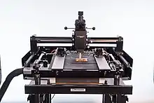
Mechanical probe station
A mechanical probe station is used to physically acquire signals from the internal nodes of a semiconductor device. The probe station utilizes manipulators which allow the precise positioning of thin needles on the surface of a semiconductor device. If the device is being electrically stimulated, the signal is acquired by the mechanical probe and is displayed on an oscilloscope or SMU. The mechanical probe station is often used in the failure analysis of semiconductor devices.
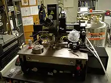
There are two types of mechanical probes: active and passive. Passive probes usually consist of a thin tungsten needle. Active probes utilize a FET device on the probe tip in order to significantly reduce loading on the circuit.
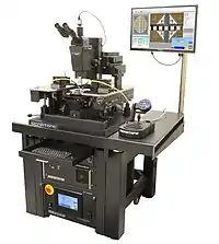 Microworld Semi-automatic probing stations for full wafer characterization
Research
Mechanical probe stations are often used in academic research on electronics and materials science. It is often faster and more flexible to test a new electronic device or sample with a probe station than to wire bond and package the device before testing.
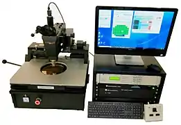
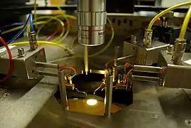 Close-up of passive probes on the same probe station
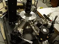 This Desert Cryogenics probe station encloses the sample and probes in a vacuum chamber and permits the introduction of cryogens to cool the sample to low temperatures.
Probe stations initially were designed to manage micron level semiconductor wafer testing. It is still a huge part of the testing that goes on but as Moore's Law has reduced the sizes of semiconductor devices over time. Probe stations have evolved to better manage both wafer level and device testing. An example of this is the VERSA probe system by Micromanipulator. Systems like the VERSA can visualize and probe all size wafers from 50mm, 100mm, 150mm, 200mm, 300mm, and even 450mm. systems like the VERSA can also manage testing individual chips or die as well as large +24" application boards with decapsulated parts.
