Metal assisted chemical etching
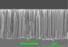
Metal Assisted Chemical Etching (also known as MACE) is the process of wet chemical etching of semiconductors (mainly silicon) with the use of a metal catalyst, usually deposited on the surface of a semiconductor in the form of a thin film or nanoparticles. The semiconductor, covered with the metal is then immersed in an etching solution containing and oxidizing agent and hydrofluoric acid. The metal on the surface catalyzes the reduction of the oxidizing agent and therefore in turn also the dissolution of silicon. In the majority of the conducted research this phenomenon of increased dissolution rate is also spatially confined, such that it is increased in close proximity to a metal particle at the surface. Eventually this leads to the formation of straight pores that are etched into the semiconductor (see figure to the right). This means that a pre-defined pattern of the metal on the surface can be directly transferred to a semiconductor substrate.[1]

History of development
MACE is a relatively new technology in semiconductor engineering and therefore it has yet to be a process that is used in industry. The first attempts of MACE consisted of a silicon wafer that was partially covered with aluminum and then immersed in an etching solution.[2] This material combination led to an increased etching rate compared to bare silicon. Often this very first attempt is also called galvanic etching instead of metal assisted chemical etching.
Further research showed that a thin film of a noble metal deposited on a silicon wafer's surface can also locally increase the etching rate. In particular, it was observed that noble metal particles sink down into the material when the sample is immersed in an etching solution containing an oxidizing agent and hydrofluoric acid (see image in the introduction).[3] This method is now commonly called the metal assisted chemical etching of silicon. Other semiconductors were also successfully etched with MACE, such as silicon carbide[4] or gallium nitride.[5] However, the main portion of research is dedicated to MACE of silicon.
It has been shown that both noble metals such as gold,[6] platinum,[7] palladium, [8] and silver,[9] and base metals such as iron,[10] nickel,[11][12] copper,[13] and aluminium[14] can act as a catalyst in the process.
Theory

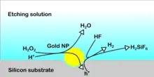
Some elements of MACE are commonly accepted in the scientific community, while others are still under debate.[1] There is agreement that the reduction of the oxidizing agent is catalyzed by the noble metal particle (see figure to the left). This means that the metal particle has a surplus of positive charge which is eventually transferred to the silicon substrate. Each of the positive charges in the substrate can be identified as a hole (h+) in the valence band of the substrate, or in more chemical terms it may be interpreted as a weakened Si-Si bond due to the removal of an electron. The weakened bonds can be attacked by a nucleophilic species such as HF or H2O, which in turn leads to the dissolution of the silicon substrate in close proximity to the noble metal particle.
From a thermodynamic point of view, the MACE process is possible because the redox potential of the redox couple corresponding to the used oxidizing agents (hydrogen peroxide or potassium permanganate) are below the valence band edge at the electrochemical energy scale. Equivalently, one could say that the electrochemical potential of the electron in the etching solution (due to the presence of oxidizing agent) is lower than the electrochemical potential of the electron in the substrate, hence electrons are removed from the silicon. In the end, this accumulation of positive charge leads to the dissolution of the substrate by hydrofluoric acid.[1]
MACE consists of multiple individual reactions. At the metal particle, the oxidizing agent is reduced. In the case of hydrogen peroxide this can be written down as follows:
The created holes (h+) are then consumed during the dissolution of silicon. There are several possible reactions via which the dissolution can take place, but here just one example is given:
There are still some unclear aspects of the MACE process. The model proposed above requires contact of the metal particle with the silicon substrate which is somehow conflicting with the etching solution being underneath the particle. This can be explained with a dissolution and redeposition of metal during MACE. In particular it is proposed, that some metal ions from the particle are dissolved and eventually are re-deposited at the silicon surface with a redox reaction. In this case the metal particle (or even larger noble metal thin films) could partially maintain contact to the substrate while also etching could partially take place underneath the metal.[15]
It is also observed that in the vicinity of straight pores as shown in the introduction also a micro-porous region between the pores is formed. Generally this is attributed to holes that diffuse away from the particle and hence contribute to etching at more distant locations.[16] This behavior is dependent on the doping type of substrate as well as on the type of noble metal particle. Therefore, it is proposed that the formation of such a porous region beneath the straight pores depends on the type of barrier that is formed at the metal/silicon interface. In the case of an upward band bending the electric field in the depletion layer would point towards the metal. Therefore, holes cannot diffuse further into the substrate and thus no formation of a micro-porous region is observed. In the case of downward band-bending holes could escape into the bulk of the silicon substrate and eventually lead to etching there.[17]
Experimental procedure of MACE

As already stated above MACE requires metal particles or a thin metal thin film on top of a silicon substrate. This can be achieved with several methods such as sputter deposition or thermal evaporation.[18] A method to obtain particles from a continuous thin film is thermal dewetting.[19] These deposition methods can be combined with lithography[20] such that only desired regions are covered with metal. Since MACE is an anisotropic etching method (etching takes place not in all spatial directions) a pre-defined metal pattern can be directly transferred into the silicon substrate. Another method of depositing metal particles or thin films is electroless plating of noble metals on the surface of silicon. Since the redox potentials of the redox couples of noble metals are below the valence band edge of silicon, noble metal ions can (like described in the theory section) inject holes (or extract electrons) from the substrate while they are reduced. In the end metallic particles or films are obtained at the surface.[21] Finally, after the deposition of the metal on the surface of silicon, the sample is immersed in an etching solution containing hydrofluoric acid and oxidizing agent. Etching will take place as long as the oxidizing agent and the acid are consumed or until the sample is removed from the etching solution.
Applications of MACE

The reason why MACE is heavily researched is that it allows completely anisotropic etching of silicon substrates which is not possible with other wet chemical etching methods (see figure to the right). Usually the silicon substrate is covered with a protective layer such as photoresist before it is immersed in an etching solution. The etching solution usually has no preferred direction of attacking the substrate, therefore isotropic etching takes place. In semiconductor engineering, however it is often required that the sidewalls of the etched trenches are steep. This is usually realized with methods that operate in the gas-phase such as reactive ion etching. These methods require expensive equipment compared to simple wet etching. MACE, in principle allows the fabrication of steep trenches but is still cheap compared to gas-phase etching methods.
Porous silicon
Metal assisted chemical etching allows for the production of porous silicon with photoluminescence.[3]
Black silicon
Black silicon is silicon with a modified surface and is a type of porous silicon. There are several works on obtaining black silicon using MACE technology. The main application of black silicon is solar energy.[11][12]
Black Gallium Arsenide
Black Gallium Arsenide with light trapping properties have been also produced by MACE.[22]
References
- Huang, Zhipeng; Geyer, Nadine; Werner, Peter; de Boor, Johannes; Gösele, Ulrich (11 January 2011). "Metal‐Assisted Chemical Etching of Silicon: A Review: In memory of Prof. Ulrich Gösele". Advanced Materials. 23 (2): 285–308. doi:10.1002/adma.201001784.
- Dimova-Malinovska, D; Sendova-Vassileva, M; Tzenov, N; Kamenova, M (April 1997). "Preparation of thin porous silicon layers by stain etching". Thin Solid Films. 297 (1–2): 9–12. doi:10.1016/S0040-6090(96)09434-5.
- Li, X.; Bohn, P. W. (16 October 2000). "Metal-assisted chemical etching in HF/H2O2 produces porous silicon". Applied Physics Letters. 77 (16): 2572–2574. doi:10.1063/1.1319191.
- Leitgeb, Markus; Zellner, Christopher; Schneider, Michael; Schwab, Stefan; Hutter, Herbert; Schmid, Ulrich (1 November 2017). "Metal assisted photochemical etching of 4H silicon carbide". Journal of Physics D: Applied Physics. 50 (43): 435301. doi:10.1088/1361-6463/aa8942.
- Dı́az, Diego J.; Williamson, Todd L.; Adesida, Ilesanmi; Bohn, Paul W.; Molnar, Richard J. (15 December 2003). "Morphology evolution and luminescence properties of porous GaN generated via Pt-assisted electroless etching of hydride vapor phase epitaxy GaN on sapphire". Journal of Applied Physics. 94 (12): 7526–7534. doi:10.1063/1.1628833.
- Mikhael, Bechelany; Elise, Berodier; Xavier, Maeder; Sebastian, Schmitt; Johann, Michler; Laetitia, Philippe (26 October 2011). "New Silicon Architectures by Gold-Assisted Chemical Etching". ACS Applied Materials & Interfaces. 3 (10): 3866–3873. doi:10.1021/am200948p.
- Tsujino, Kazuya; Matsumura, Michio (2005). "Helical Nanoholes Bored in Silicon by Wet Chemical Etching Using Platinum Nanoparticles as Catalyst". Electrochemical and Solid-State Letters. 8 (12): C193. doi:10.1149/1.2109347.
- Chen, Jun-Ming; Chen, Chia-Yuan; Wong, C.P.; Chen, Chia-Yun (January 2017). "Inherent formation of porous p-type Si nanowires using palladium-assisted chemical etching". Applied Surface Science. 392: 498–502. doi:10.1016/j.apsusc.2016.09.048.
- Lee, Jung-In; Park, Soojin (January 2013). "High-performance porous silicon monoxide anodes synthesized via metal-assisted chemical etching". Nano Energy. 2 (1): 146–152. doi:10.1016/j.nanoen.2012.08.009.
- Loni, A.; Barwick, D.; Batchelor, L.; Tunbridge, J.; Han, Y.; Li, Z. Y.; Canham, L. T. (1 May 2011). "Extremely High Surface Area Metallurgical-Grade Porous Silicon Powder Prepared by Metal-Assisted Etching". Electrochemical and Solid-State Letters. 14 (5): K25–K27. doi:10.1149/1.3548513.
- Volovlikova, Olga V.; Gavrilov, S.A.; Lazarenko, P.I.; Kukin, A.V.; Dudin, A.A.; Tarhanov, A.K. (June 2019). "Influence of Etching Regimes on the Reflectance of Black Silicon Films Formed by Ni-Assisted Chemical Etching". Key Engineering Materials. 806: 24–29. doi:10.4028/www.scientific.net/KEM.806.24.
- Azeredo, B P; Sadhu, J; Ma, J; Jacobs, K; Kim, J; Lee, K; Eraker, J H; Li, X; Sinha, S; Fang, N; Ferreira, P; Hsu, K (7 June 2013). "Silicon nanowires with controlled sidewall profile and roughness fabricated by thin-film dewetting and metal-assisted chemical etching". Nanotechnology. 24 (22): 225305. doi:10.1088/0957-4484/24/22/225305.
- Qiu, Teng; Chu, Paul K. (May 2008). "Self-selective electroless plating: An approach for fabrication of functional 1D nanomaterials". Materials Science and Engineering: R: Reports. 61 (1–6): 59–77. doi:10.1016/j.mser.2008.03.001.
- Uddin, Shahnawaz; Hashim, Md Roslan; Pakhuruddin, Mohd Zamir (June 2021). "Aluminium-assisted chemical etching for fabrication of black silicon". Materials Chemistry and Physics. 265: 124469. doi:10.1016/j.matchemphys.2021.124469.
- Geyer, Nadine; Fuhrmann, Bodo; Huang, Zhipeng; de Boor, Johannes; Leipner, Hartmut S.; Werner, Peter (21 June 2012). "Model for the Mass Transport during Metal-Assisted Chemical Etching with Contiguous Metal Films As Catalysts". The Journal of Physical Chemistry C. 116 (24): 13446–13451. doi:10.1021/jp3034227.
- Li, Xiuling (April 2012). "Metal assisted chemical etching for high aspect ratio nanostructures: A review of characteristics and applications in photovoltaics". Current Opinion in Solid State and Materials Science. 16 (2): 71–81. doi:10.1016/j.cossms.2011.11.002.
- Lai, Ruby A.; Hymel, Thomas M.; Narasimhan, Vijay K.; Cui, Yi (13 April 2016). "Schottky Barrier Catalysis Mechanism in Metal-Assisted Chemical Etching of Silicon". ACS Applied Materials & Interfaces. 8 (14): 8875–8879. doi:10.1021/acsami.6b01020.
- Kabalan, Amal. "A Comparative Study on the Effects of Passivation Methods on the Carrier Lifetime of RIE and MACE Silicon Micropillars." Applied Sciences 9.9 (2019): 1804.
- Backes, A., et al. "Influence of metallic catalyst and doping level on the metal assisted chemical etching of silicon." Scripta Materialia 114 (2016): 27-30.
- Chang, Shih‐Wei, et al. "Densely packed arrays of ultra‐high‐aspect‐ratio silicon nanowires fabricated using block‐copolymer lithography and metal‐assisted etching." Advanced functional materials 19.15 (2009): 2495-2500.
- Smith, Zachary R., Rosemary L. Smith, and Scott D. Collins. "Mechanism of nanowire formation in metal assisted chemical etching." Electrochimica Acta 92 (2013): 139-147.
- Lova, Paola; Robbiano, Valentina; Cacialli, Franco; Comoretto, Davide; Soci, Cesare (2018). "Black GaAs by Metal-Assisted Chemical Etching". ACS Applied Materials & Interfaces. 10 (39): 33434–33440. doi:10.1021/acsami.8b10370. PMID 30191706.