Multi-tip scanning tunneling microscopy
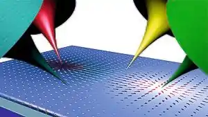
Multi-tip scanning tunneling microscopy (Multi-tip STM) extends scanning tunneling microscopy (STM) from imaging to dedicated electrical measurements at the nanoscale like a ″multimeter at the nanoscale″. In materials science, nanoscience, and nanotechnology, it is desirable to measure electrical properties at a particular position of the sample. For this purpose, multi-tip STMs in which several tips are operated independently have been developed. Apart from imaging the sample, the tips of a multi-tip STM are used to form contacts to the sample at desired locations and to perform local electrical measurements.
Introduction
As microelectronics evolves into nanoelectronics, it is essential to perform electronic transport measurements at nanoscale. The standard approach is to use lithographic methods to contact nanostructures, as it is also used in the final nanoelectronic device. In research and development stages, however, other methods to contact nanoelectronic devices or generally nanostructures may be more suitable. An alternative approach for contacting nanostructures uses the tips of a multi-tip scanning tunneling microscope—in analogy to the test leads of a multimeter used at macroscale. The advantages of this approach are: (a) in situ contacting of ″as grown″ nanostructures still under vacuum helps keep delicate nanostructures free from contamination induced by lithography steps performed for contacting. (b) Flexible positioning of the contacting tips and different contact configurations are easy to realize, while lithographic contacts are fixed. (c) Probing with sharp tips can be non-invasive (high ohmic), while lithographic contacts are typically invasive (low ohmic).[1] To use a scanning tunneling microscope (STM) for electrical transport measurements at nanostructures or at surfaces, more than one tip is required. This motivates the use of multi-tip scanning tunneling microscopes which give access to the above outlined advantages in nanoprobing. Several review articles about multi-tip STM can be found in the further reading section below.
Principle of operation
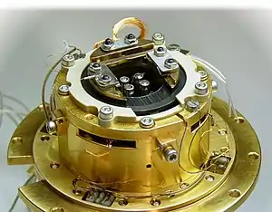
Multi-tip scanning tunneling microscopes consist usually of four STM units positioning each of the tips individually to the desired position on the sample. To reduce thermal drift of the tips, the four STM units, should be as small and compact as possible. It is important that the motion of the tips can be observed, either by an optical microscope, or by a scanning electron microscope (SEM). This allows to bring the tips close together and to position them at the desired measurement locations. The tips in a multi tip STM are usually mounted under 45° relative to the vertical direction to facilitate positioning all tips at one region on the sample.
After the first multi-tip STM was introduced,[2] several home-built instruments were designed and today, several commercial instruments are available as well.
An extension of the multi-tip STM technique is the upgrade to atomic force microscopy (AFM) operation. For applications in nanoelectronics, most of the samples consist of conducting "target" areas at the surface, separated by non-conducting areas. To guide the tip to the conducting areas, AFM imaging instead of or in addition to optical microscope or SEM guided positioning of the tips, can be very useful.[3]

When performing electrical measurements on the nanoscale, it should be stressed that the contact resistance is often very large at the STM tip contact to the sample because the contact area is very small, so that four-point measurements are indispensable in resistance measurements with a muti-tip STM. This is even more important in measuring nano-scale objects, because the contacts to these objects are inevitably nano-scale. In a two-point resistance measurement, the two current injecting tips are used for voltage probing as well. Therefore, the measured resistance R = V/I also includes the contribution from the two contact resistances RC. In a four-point measurement the current injecting circuit is separated from the voltage sensing circuit. If the voltage measurement is performed with a large internal resistance RV, the influence of the contact resistances can be neglected. This is the main advantage of the four-point measurement.

Performing electrical measurements with a multi-tip STM demands more than four tips and the ability to position them as required. Concerted measurements of currents and voltages with all four tips must be performed. The electronics allows operating each tip either as (biased) current probe, or as voltage probe. Different I-V ramps are applied between different tips (and/or the sample). In the simplest case a current is injected between the two outer tips and a potential difference is measured between the inner tips (classical four-point measurement), also as a function of temperature. [4] However, also various kinds of other measurements can be performed, e.g., a tip or the sample can be used as gate electrode.
Applications of multi-tip STM
Graphene nanoribbons and graphene nanostructures
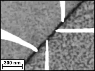
The local transport properties of 40 nm wide graphene nanoribbons grown on silicon carbide (SiC) substrates, are studied by means of a multi-tip STM. The graphene nanoribbons exhibit exceptional transport properties, such as ballistic conduction even at room temperature with mean free paths up to several µm.[5] Such epitaxial graphene nanoribbons are important not only in fundamental science, but also because they can be readily produced in thousands in advanced nanoelectronics, which can make use of their room-temperature ballistic transport properties.
Resistance profiling along freestanding GaAs nanowires
The multi-tip STM can be used for resistance mapping along freestanding GaAs nanowires with a diameter of about 100 nm. The nanowires are still “as grown” upright and attached to the substrate, thus it is not possible to contact nanowires by lithographic techniques. In the measurement configuration shown in the figure, the sample is tilted by 45° to facilitate optimal SEM imaging of the nanowires. Three tips brought into contact with a nanowire realize a four-point resistance measurement (with the sample as fourth contact). Tip 1 injects the current to the nanowire with the sample acting as current drain, while tip 2 and tip 3 act as voltage probes. While it is relatively easy to study the structure of these nanowires e.g., with high resolution electron microscopy, it is difficult to access the electrical properties determined by the doping profile along the nanowire. From the measuremed four-point resistance along the nanowire a doping profile along the nanowire can be obtained.[6][7][8]
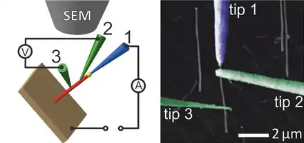 Left: Schematic of a four-point measurement on a nanowire with three tips contacting the nanowire. Right: SEM image of a freestanding nanowire contacted by three tips. The STM tips act like the test leads of a multimeter, however, contacting objects like the nanowire at the nanoscale. |
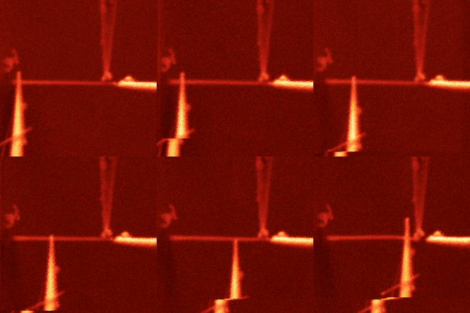 Movie of an STM tip moving along a GaAs nanowire measuring a four-point probe resistance profile at many points along the nanowire. |
Multi-tip potentiometry
A method giving valuable insight into the charge transport properties of nanostructures is the scanning tunneling potentiometry (STP).[9] STP can be performed with a multi-tip STM and allows to map the potential landscape while a current flows through the film, nanostructure, or surface under study. Potentiometry maps give insight into fundamental transport properties, such as the influence of defects on the local electric transport. The implementation is shown in the figure, with the outer tips injecting a current into the nanostructure or surface being studied, while then center tip simultaneously measures the topography and also records the electric potential at each image point which is induced by the flowing current. This way a potential map measured e.g. on a silicon surface can be acquired with a potential resolution is a couple of µV. The potential map in the figure shows that the largest potential drop occurs at the atomic step edges. From these data the resistance of a single atomic step, or a domain boundary can be obtained. Moreover, if a current flows around a nanoscale defect like. e.g.. a void, the potential map developing due to the flowing current can be measured.[10]
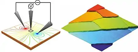 Left: Schematic of the scanning tunneling potentiometry setup implemented into the multi-tip scanning tunneling microscope. Two tips inject a current in the sample surface with the third tip mapping the resulting potential distribution. The scan area is indicated as a black square. Right: Potential map measured on a Si surface with the main potential drop occurring at the atomic step edges. The current flows from the top to the bottom in this image. |
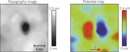 Left: STM topography image of a 5 nm large void in a topological insulator film. Right: Potential dipole developing around the nanscale void due to the current flowing. |
Disentangling surface conductivity from bulk conductivity
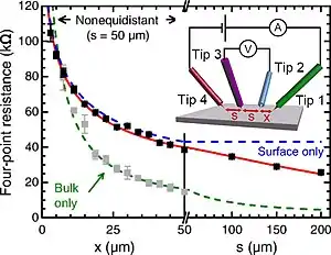
As nano-devices become smaller and smaller, the surface to volume ratio (i.e., the fraction of atoms located at the surface) increases constantly. The increasing importance of surface conductance compared to conductance through the bulk in modern nanoelectronic devices calls for a reliable determination of the surface conductivity to minimize the influence of undesired leakage currents on the device performance or to use surfaces as functional units. A model system for corresponding investigations is the Si(111)-7×7 surface. The challenge is to disentangle the contribution due to the surface conductivity from the bulk conductivity. Using multi-tip STM, researchers developed a method that uses distance dependent four-probe measurements in the linear configuration to determine surface conductivity.[4][11][12]
Spin current in quantum materials
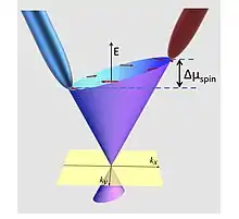
Multi-tip STM is used as a method for the detection of the spin-voltage in topological insulators using spin-polarized four-probe scanning tunneling microscopy on Bi2Te2Se surfaces. The spin-dependent electrochemical potential is separated from the ohmic contribution. This component is identified as the spin-chemical potential arising from the 2D charge current through the spin momentum locked topological surface states (TSS). The new method uses a magnetic tip to observe the spin behavior of electrons on the material's surface.[13]
See also
References
- Voigtländer, B; Cherepanov, V; Korte, S; Leis, A; Cuma, D; Just, S & Lüpke, F (2018). "Invited Review Article: Multi-tip scanning tunneling microscopy: Experimental techniques and data analysis". Review of Scientific Instruments. 89 (10): 101101. doi:10.1063/1.5042346. PMID 30399776.
- Shiraki, I; Tanabe, F; Hobara, R; Nagao, T & Hasegawa, S (2001). "Independently driven four-tip probes for conductivity measurements in ultrahigh vacuum". Surf. Sci. 493 (1–3): 633–643. doi:10.1016/S0039-6028(01)01276-6.
- Higuchi, S; Kubo, O; Kuramochi, H; Aono, M & Nakayama, T (2011). "A quadruple-scanning-probe force microscope for electrical property measurements of microscopic materials". Nanotechnology. 22 (28): 285205. doi:10.1088/0957-4484/22/28/285205. PMID 21659691.
- Gerasimenko, Y; Vaskivskyi, I; Liskevich, M; Ravnik, J; Vodeb, J; Diego, M; Kabanov, V & Mihailovic, D (2019). "Quantum jamming transition to a correlated electron glass in 1T-TaS2". Nature Materials. 317: 505. arXiv:1803.00255. doi:10.1038/s41563-019-0423-3.
- Baringhaus, J; Ruan, M; Edler, F; Tejeda, A; Sicot, M; Taleb-Ibrahimi, A; Li, A-P; Jiang, Z; Conrad, EH; Berger, C; Tegenkamp, C & de Heer, WA (2014). "Exceptional ballistic transport in epitaxial graphene nanoribbons". Nature. 506 (7488): 349–354. arXiv:1301.5354. doi:10.1038/nature12952. PMID 24499819. S2CID 4445858.
- Korte, S; Steidl, M; Prost, W; Cherepanov, V; Voigtländer, B; Zhao, W; Kleinschmidt, P & Hannappel, T (2013). "Resistance and dopant profiling along freestanding GaAs nanowires". Applied Physics Letters. 103 (14): 143104. doi:10.1063/1.4823547.
- Nägelein, A; Liborius, L; Steidl, M; Blumberg, C; Kleinschmidt, P; Poloczek, A & Hannappel, T (2017). "Comparative analysis on resistance profiling along tapered semiconductor nanowires: multi-tip technique versus transmission line method". Journal of Physics: Condensed Matter. 29 (39): 394007. doi:10.1088/1361-648X/aa801e. PMID 28714857.
- Nägelein, A; Steidl, M; Korte, S; Voigtländer, B; Prost, W; Kleinschmidt, P & Hannappel, T (2018). "Investigation of charge carrier depletion in freestanding nanowires by a multi-probe scanning tunneling microscope". Nano Research. 11 (11): 5924–5934. doi:10.1007/s12274-018-2105-x. S2CID 139202364.
- Lüpke, F; Korte, S; Cherepanov, V & Voigtländer, B (2015). "Scanning tunneling potentiometry implemented into a multi-tip setup by software". Review of Scientific Instruments. 86 (12): 123701. arXiv:1508.07717. doi:10.1063/1.4936079. PMID 26724036. S2CID 2239279.
- Lüpke, F; Eschbach, M; Heider, T; Lanius, M; Schüffelgen, P; Rosenbach, D; von den Driesch, N; Cherepanov, V; Mussler, G; Plucinski, L; Grützmacher, D; Schneider, CM & Voigtländer, B (2017). "Electrical resistance of individual defects at a topological insulator surface". Nature Communications. 8: 15704. arXiv:1704.06580. doi:10.1038/ncomms15704. PMC 5472778. PMID 28604672.
- Just, S; Blab, M; Korte, S; Cherepanov, V; Soltner, H & Voigtländer, B (2015). "Surface and Step Conductivities on Si(111) Surfaces". Physical Review Letters. 115 (6): 066801. doi:10.1103/PhysRevLett.115.066801. PMID 26296126.
- Just, S; Soltner, H; Korte, S; Cherepanov, V & Voigtländer, B (2017). "Surface conductivity of Si(100) and Ge(100) surfaces determined from four-point transport measurements using an analytical N-layer conductance model". Physical Review B. 95 (7): 075310. arXiv:1610.02239. doi:10.1103/PhysRevB.95.075310. S2CID 118383531.
- Hus, SM; Zhang, X-G; Nguyen, GD; Ko, W; Baddorf, AP; Chen, YP & Li, A-P (2017). "Detection of the Spin-Chemical Potential in Topological Insulators Using Spin-Polarized Four-Probe STM". Physical Review Letters. 119 (13): 137202. doi:10.1103/PhysRevLett.119.137202. PMID 29341679.
Further reading
- Hofmann, P & Wells, JW (2009). "Surface sensitive conductance measurements". J. Phys. Condens. Matter. 21 (1): 013003. doi:10.1088/0953-8984/21/1/013003. PMID 21817212.
- Nakayama, T; Kubo, O; Shingaya, Y; Higuchi, S; Hasegawa, T; Jiang, C; Okuda, T; Kuwahara, Y; Takami, K & Aono, M (2012). "Development and application of multiple‐probe scanning probe microscopes". Adv. Mater. 24 (13): 1675–1692. doi:10.1002/adma.201200257. PMID 22378596.
- Li, A-P; Clark, KW; Zhang, X & Baddorf, AP (2013). "Electron transport at the nanometer‐scale spatially revealed by four‐probe scanning tunneling microscopy". Adv. Funct. Mater. 23 (20): 2509–2524. doi:10.1002/adfm.201203423.
- Xu, T & Grandidier, B. (2015). Electrical characterization of semiconductor nanowires by scanning-probe microscopy, in: Semiconductor Nanowires - Materials, Synthesis, Characterization and Applications, Ed.: J. Arbiol and Q. Xiong, Elsevier. p. 277. ISBN 978-1-78242-253-2.
- Nakayama, T; Shingaya, Y & Aono, M (2016). "Multiple-probe scanning probe microscopes for nanoarchitectonic materials science". Jpn. J. Appl. Phys. 55 (11): 1102A7. doi:10.7567/JJAP.55.1102A7.