Nanolaser
A nanolaser is a laser that has nanoscale dimensions and it refers to a micro-/nano- device which can emit light with light or electric excitation of nanowires or other nanomaterials that serve as resonators. A standard feature of nanolasers includes their light confinement on a scale approaching or suppressing the diffraction limit of light. These tiny lasers can be modulated quickly and, combined with their small footprint, this makes them ideal candidates for on-chip optical computing.
History
Albert Einstein proposed the stimulated emission in 1916,[1][2] which contributed to the first demonstration of laser in 1961.[2][3] From then on, people have been pursuing the miniaturization of lasers for more compact size and less energy consumption all the time. Since people noticed that light has different interactions with matter at the nanoscale in the 1990s, significant progress has been made to achieve the miniaturization of lasers and increase power conversion efficiency. Various types of nanolasers have been developed over the past decades.
In the 1990s, some intriguing designs of microdisk laser[4][5] and photonic crystal laser[6][7] were demonstrated to have cavity size or energy volume with micro-/nano- diameters and approach the diffraction limit of light. Photoluminescence behavior of bulk ZnO nanowires was first reported in 2001 by Prof. Peidong Yang from the University of California, Berkeley and it opened the door to the study of nanowire nanolasers.[8] These designs still do not exceed the diffraction limit until the demonstration of plasmonic lasers or spasers.
David J. Bergman and Mark Stockman first proposed amplified surface plasmon waves by stimulated emission and coined the term spaser as "surface plasmon amplification by stimulated emission of radiation" in 2003.[9][10] Until 2009, the plasmonic nanolasers or spasers were first achieved experimentally,[11][12][13] which were regarded as the smallest nanolasers at that time.
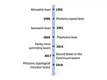
Since roughly 2010, there has been progress in nanolaser technology, and new types of nanolasers have been developed, such as parity-time symmetry laser, bound states in the continuum laser and photonic topological insulators laser.[14]
Comparison with conventional lasers
While sharing many similarities with standard lasers, nanolasers maintain many unique features and differences from the conventional lasers due to the fact that light interacts differently with matter at the nanoscale.
Mechanism
Similar to the conventional lasers, nanolasers also based on stimulated emission which was proposed by Einstein;[1][2][3] the main difference between nanolaser and the conventional ones in mechanism is light confinement. The resonator or cavity plays an important role in selecting the light with a certain frequency and the same direction as the most priority amplification and suppressing the other light to achieve the confinement of light. For conventional lasers, Fabry–Pérot cavity with two parallel reflection mirrors is applied. In this case, light could be confined to a maximum of half its wavelength and such limit is deemed the diffraction limit of light.[15] To approach or decrease the diffraction limit of light, one way is to improve the reflectivity of gain medium, such as using photonic bandgap and nanowires. Another effective way to exceed the diffraction limit is to convert light into surface plasmons in nanostructuralized metals, for amplification in cavity.[14][16] Recently, new mechanisms of strong light confinement for nanolasers including parity–time symmetry,[17] photonic topological insulators,[18][19] and bound states in the continuum[20] have been proposed.
Properties
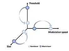
Compared with conventional lasers, nanolasers show distinct properties and capabilities. The biggest advantages of nanolasers are their ultra-small physical volumes to improve energy efficiencies, decrease lasing thresholds, and achieve high modulation speeds.[21][22][23]
Types of nanolasers
Microdisk laser
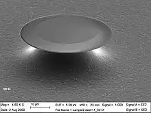
A microdisk laser is a very small laser consisting of a disk with quantum well structures built into it. Its dimensions can exist on the micro-scale or nano-scale. Microdisk lasers use a whispering-gallery mode resonant cavity.[4][5][25] The light in cavity travels around the perimeter of the disk and the total internal reflection of photons can result in a strong light confinement and a high quality factor, which means a powerful ability of the microcavity to store the energy of photons coupled into the cavity.
Photonic crystal laser
Photonic crystal lasers utilize periodic dielectric structures with different refractive indices; light can be confined with the use of a photonic crystal microcavity. In dielectric materials, there is orderly spatial distribution. When there is a defect in the periodic structure, the two-dimensional or three-dimensional photonic crystal structure will confine the light in the space of the diffractive limit and produce the Fano resonance phenomenon, which means a high quality factor with a strong light confinement for lasers. The fundamental feature of photonic crystals is the photonic bandgap, that is, the light whose frequency falls in the photonic band gap cannot propagate in the crystal structure, thus resulting in a high reflectivity for incident light and a strong confinement of light to a small volume of wavelength scale.[6][13][26] The appearance of photonic crystals makes the spontaneous emission in the photon gap completely suppressed. But the high cost of photonic crystal impedes the development and spreading applications of photonic crystal lasers.
Nanowire laser
.jpg.webp)
Semiconductor nanowire lasers have a quasi-one-dimensional structure with diameters ranging from a few nanometers to a few hundred nanometers and lengths ranging from hundreds of nanometers to a few microns. The width of nanowires is large enough to ignore the quantum size effect, but they are high quality one-dimensional waveguides with cylindrical, rectangular, trigonal, and hexagonal cross-sections. The quasi-one-dimensional structure and high reflectivity of nanowire laser makes it have good optical waveguide and the ability of light confinement. Nanowire lasers are similar to Fabry–Pérot cavity in mechanism.[28] High reflectivity of nanowire and flat end facets of the wire constitute a good resonant cavity, in which photons can be bound between the two ends of the nanowire to limit the light energy to the axial direction of the nanowire, thus meeting the conditions for laser formation.[8][29][30][31] Polygonal nanowires can form a nearly circular cavity in cross section that supports whispering-gallery mode.
Plasmonic nanolaser

Nanolaser based on surface plasmon is known as plasmonic nanolaser, whose size far exceeds the diffraction limit of light. Especially, if a plasmonic nanolaser is nanoscopic in three dimensions, it is also called as spaser, which is known to have the smallest cavity size and mode size. Design of plasmonic nanolaser has become one of the most effective technology methods for laser miniaturization at present.[32] A little bit different from the conventional lasers, a typical configuration of plasmonic nanolaser includes a process of energy transfer to convert photons into surface plasmons.[10] In plasmonic nanolaser or spaser, the exciton is not photons anymore but surface plasmon polariton. Surface plasmons are collective oscillations of free electrons on metal surfaces under the action of external electromagnetic fields.[14][16] According to their manifestations, the cavity mode in plasmonic nanolasers can be divided into the propagating surface plasmon polaritons (SPPs) and the non-propagating localized surface plasmons (LSPs).
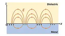
SPPs are electromagnetic waves that propagate along the interface between metal and medium, and their intensities decay gradually in the direction perpendicular to the propagation interface. In 2008, Oulton experimentally validated a plasma nanowire laser consisting of a thin dielectric layer with a low reflectivity growing on a metal surface and a gain layer with a high refractive index semiconductor nanowire.[12] In this structure, the electromagnetic field can be transferred from the metal layer to the intermediate gap layer, so that the mode energy is highly concentrated, thus greatly reducing the energy loss in the metal.
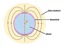
The LSP mode exists in a variety of different metal nanostructures, such as metal nanoparticles (nanospheres, nanorods, nanocubes, etc.) and arrays of nanoparticles.[32] Unlike the propagating surface plasmon polaritons, the localized surface plasmon does not propagate along the surface, but oscillates back and forth in the nanostructure in the form of standing waves. When light is incident to the surface of a metal nanoparticles, it causes a real displacement of the surface charge relative to the ions. The attraction between electrons and ions allows for the oscillation of electrode cloud and the formation of local surface from polarization excimer.[33] The oscillation of electrons is determined by the geometrical boundaries of different metal nanoparticles. When its resonance frequency is consistent with the incident electromagnetic field, it will form the localized surface plasmon resonance. In 2009, Mikhail A. Noginov of Norfolk State University in the United States successfully verified the LSPs-based nanolaser for the first time.[11] The nanolaser in this paper was composed of an Au core providing the plasmon mode and a silicon dioxide doped with OG-488 dye providing the gain medium. The diameter of the Au core was 14 nm, the thickness of the silica layer was 15 nm, and the diameter of the whole device was only 44 nm, which was the smallest nanolaser at that time.
New types of nanolasers
In addition, there have been some new types of nanolasers developed in recent years to approach the diffraction limit. Parity-time symmetry is related to a balance of optical gain and loss in a coupled cavity system. When the gain–loss contrast and coupling constant between two identical, closely located cavities are controlled, the phase transition of lasing modes occurs at an exceptional point.[34] Bound states in the continuum laser confines light in an open system via the elimination of radiation states through destructive interference between resonant modes.[13][20] A photonic topological insulator laser is based on topological insulators optical mode, where the topological states is confined within the cavity boundaries and they can be used for the formation of laser.[35] All of those new types of nanolasers have high quality factor and can achieve cavity size and mode size approaching the diffraction limit of the light.
Applications
Due to the unique capabilities including low lasing thresholds, high energy efficiencies and high modulation speeds, nanolasers show great potentials for practical applications in the fields of materials characterization, integrated optical interconnects, and sensing.
Nanolasers for material characterization
The intense optical fields of such a laser also enable the enhancement effect in non-linear optics or surface-enhanced-raman-scattering (SERS).[36] Nanowire nanolasers can be capable of optical detection at the scale of a single molecule with high resolution and ultrafast modulation.
Nanolasers for integrated optical interconnects
Internet is developing at an extremely high speed with large energy consumption for data communication. The high energy efficiency of nanolasers plays an important role in decreasing energy consumption for future society.[37][38]
Nanolasers for sensing
Plasmonic nanolaser sensors have recently been demonstrated that can detect specific molecules in air and be used for optical biosensors. Molecules can modify the surface of metal nanoparticles and impact the surface recombination velocity of gain medium of a plasmonic nanolaser, which contributes to the sensing mechanism of plasmonic nanolasers.[22][39]
Challenges
Although nanolasers have shown great potential, there are still some challenges towards the large-scale use of nanolasers, for example, electrically injected nanolasers, cavity configuration engineering and metal quality improvement.[22][40] For nanolasers, the realization of electrically injected or pumped operation at room temperature is a key step towards its practical application. However, most nanolaser are optically pumped and the realization of electrically injected nanolasers is still a main technical challenge at present.[40] Only a few studies have reported electrically injected nanolasers. Moreover, it still remains a challenge to realize cavity configuration engineering and metal quality improvement, which are crucial to satisfy the high-performance requirement of nanolasers and achieve their applications.[41] Recently, nanolaser arrays show great potential to increase the power efficiency and accelerate modulation speed.[42]
See also
- List of laser articles
- Laser
- Spaser, plasmonic laser
- Polariton laser
- Nanowire laser
References
- Masters, Barry R. (2012). "Albert Einstein and the Nature of Light". Optics and Photonics News. 23 (7): 42–47. doi:10.1364/OPN.23.7.000042. ISSN 1541-3721.
- Gross, Andreas J.; Herrmann, Thomas R. W. (2007). "History of Lasers". World Journal of Urology. 25 (3): 217–220. doi:10.1007/s00345-007-0173-8. ISSN 1433-8726. PMID 17564717. S2CID 5650002.
- Bernard, Maurice G. A.; Duraffourg, Georges (1961). "Laser Conditions in Semiconductors". Physica Status Solidi B. 1 (7): 699–703. Bibcode:1961PSSBR...1..699B. doi:10.1002/pssb.19610010703. ISSN 1521-3951. S2CID 94232997.
- McCall, S. L.; Levi, A. F. J.; Slusher, R. E.; Pearton, S. J.; Logan, R. A. (1992). "Whispering‐Gallery Mode Microdisk Lasers". Applied Physics Letters. 60 (3): 289–291. Bibcode:1992ApPhL..60..289M. doi:10.1063/1.106688. ISSN 0003-6951.
- Frateschi, N. C.; Levi, A. F. J. (1995). "Resonant Modes and Laser Spectrum of Microdisk Lasers". Applied Physics Letters. 66 (22): 2932–2934. Bibcode:1995ApPhL..66.2932F. doi:10.1063/1.114233. ISSN 0003-6951.
- Painter, O.; Lee, R. K.; Scherer, A.; Yariv, A.; O'Brien, J. D.; Dapkus, P. D.; Kim, I. (1999). "Two-Dimensional Photonic Band-Gap Defect Mode Laser". Science. 284 (5421): 1819–1821. doi:10.1126/science.284.5421.1819. ISSN 0036-8075. PMID 10364550.
- Lončar, Marko; Yoshie, Tomoyuki; Scherer, Axel; Gogna, Pawan; Qiu, Yueming (2002). "Low-Threshold Photonic Crystal Laser". Applied Physics Letters. 81 (15): 2680–2682. Bibcode:2002ApPhL..81.2680L. doi:10.1063/1.1511538. ISSN 0003-6951.
- Huang, Michael H.; Mao, Samuel; Feick, Henning; Yan, Haoquan; Wu, Yiying; Kind, Hannes; Weber, Eicke; Russo, Richard; Yang, Peidong (2001). "Room-Temperature Ultraviolet Nanowire Nanolasers". Science. 292 (5523): 1897–1899. Bibcode:2001Sci...292.1897H. doi:10.1126/science.1060367. ISSN 0036-8075. PMID 11397941. S2CID 4283353.
- "Birth of the Nanolaser". Nature Photonics. 3 (10): 545. 2009. Bibcode:2009NaPho...3..545.. doi:10.1038/nphoton.2009.171. ISSN 1749-4893.
- Azzam, Shaimaa I.; Kildishev, Alexander V.; Ma, Ren-Min; Ning, Cun-Zheng; Oulton, Rupert; Shalaev, Vladimir M.; Stockman, Mark I.; Xu, Jia-Lu; Zhang, Xiang (2020). "Ten Years of Spasers and Plasmonic Nanolasers". Light: Science & Applications. 9 (1): 90. Bibcode:2020LSA.....9...90A. doi:10.1038/s41377-020-0319-7. ISSN 2047-7538. PMC 7248101. PMID 32509297.
- Hill, M.T.; Marell, M.; Leong, E.S.P.; Smalbrugge, B.; Zhu, Y.; Sun, M. H.; Van Veldhoven, P.J.; Geluk, E.J.; Karouta, F.; Oei, Y.; Nötzel, R.; Ning, C.Z.; Smit, M.K. (2009). "Lasing in metal-insulator-metal sub-wavelength plasmonic waveguides". Optics Express. 17 (13): 11107–11112. Bibcode:2009OExpr..1711107H. doi:10.1364/OE.17.011107. PMID 19550510.
- Noginov, M. A.; Zhu, G.; Belgrave, A. M.; Bakker, R.; Shalaev, V. M.; Narimanov, E. E.; Stout, S.; Herz, E.; Suteewong, T.; Wiesner, U. (2009). "Demonstration of a Spaser-Based Nanolaser". Nature. 460 (7259): 1110–1112. Bibcode:2009Natur.460.1110N. doi:10.1038/nature08318. ISSN 1476-4687. PMID 19684572. S2CID 4363687.
- Oulton, Rupert F.; Sorger, Volker J.; Zentgraf, Thomas; Ma, Ren-Min; Gladden, Christopher; Dai, Lun; Bartal, Guy; Zhang, Xiang (2009). "Plasmon Lasers at Deep Subwavelength Scale". Nature. 461 (7264): 629–632. Bibcode:2009Natur.461..629O. doi:10.1038/nature08364. hdl:10044/1/19116. ISSN 1476-4687. PMID 19718019. S2CID 912028.
- Jeong, Kwang-Yong; Hwang, Min-Soo; Kim, Jungkil; Park, Jin-Sung; Lee, Jung Min; Park, Hong-Gyu (2020). "Recent Progress in Nanolaser Technology". Advanced Materials. 32 (51): 2001996. Bibcode:2020AdM....3201996J. doi:10.1002/adma.202001996. ISSN 1521-4095. PMID 32945000. S2CID 221786925.
- Ning, C. Z. (2010). "Semiconductor Nanolasers". Physica Status Solidi B. 247 (4): 774–788. Bibcode:2010PSSBR.247..774N. doi:10.1002/pssb.200945436. ISSN 1521-3951. S2CID 22061437.
- Wu, Hao; Gao, Yixiao; Xu, Peizhen; Guo, Xin; Wang, Pan; Dai, Daoxin; Tong, Limin (2019). "Plasmonic Nanolasers: Pursuing Extreme Lasing Conditions on Nanoscale". Advanced Optical Materials. 7 (17): 1900334. doi:10.1002/adom.201900334. ISSN 2195-1071. S2CID 155799465.
- Feng, Liang; Wong, Zi Jing; Ma, Ren-Min; Wang, Yuan; Zhang, Xiang (2014). "Single-Mode Laser by Parity-Time Symmetry Breaking". Science. 346 (6212): 972–975. Bibcode:2014Sci...346..972F. doi:10.1126/science.1258479. ISSN 0036-8075. PMID 25414307. S2CID 6685190.
- Bandres, Miguel A.; Wittek, Steffen; Harari, Gal; Parto, Midya; Ren, Jinhan; Segev, Mordechai; Christodoulides, Demetrios N.; Khajavikhan, Mercedeh (2018). "Topological Insulator Laser: Experiments". Science. 359 (6381): eaar4005. doi:10.1126/science.aar4005. ISSN 0036-8075. PMID 29420263.
- Yang, Yihao; Gao, Zhen; Xue, Haoran; Zhang, Li; He, Mengjia; Yang, Zhaoju; Singh, Ranjan; Chong, Yidong; Zhang, Baile; Chen, Hongsheng (2019). "Realization of a Three-Dimensional Photonic Topological Insulator". Nature. 565 (7741): 622–626. arXiv:1804.03595. Bibcode:2019Natur.565..622Y. doi:10.1038/s41586-018-0829-0. hdl:10356/138225. ISSN 1476-4687. PMID 30626966. S2CID 58004995.
- Kodigala, Ashok; Lepetit, Thomas; Gu, Qing; Bahari, Babak; Fainman, Yeshaiahu; Kanté, Boubacar (2017). "Lasing Action from Photonic Bound States in Continuum". Nature. 541 (7636): 196–199. arXiv:1508.05164. Bibcode:2017Natur.541..196K. doi:10.1038/nature20799. ISSN 1476-4687. PMID 28079064. S2CID 4465627.
- Zhuge, Ming-Hua; Pan, Caofeng; Zheng, Yazhi; Tang, Jianbin; Ullah, Salman; Ma, Yaoguang; Yang, Qing (2019). "Wavelength-Tunable Micro/Nanolasers". Advanced Optical Materials. 7 (17): 1900275. doi:10.1002/adom.201900275. ISSN 2195-1071. S2CID 197148749.
- Ma, Ren-Min; Oulton, Rupert F. (2019). "Applications of Nanolasers". Nature Nanotechnology. 14 (1): 12–22. Bibcode:2019NatNa..14...12M. doi:10.1038/s41565-018-0320-y. ISSN 1748-3395. PMID 30559486. S2CID 56178072.
- Freebody, Marie. "The Ones to Watch: Nanolasers are Breaking New Ground – and Fast". www.photonics.com. Retrieved 2021-03-03.
- Shomroni, Itay (2009-08-02), English: It's a SEM picture of a microdisk resonator, about 40 um diameter, in order to create a toroid there needs to be a CO2 reflow. Later it can be used as an optical whispering gallery modes resonator., retrieved 2021-03-02
- Levi, A. F. J. (1994). "Microdisk Lasers". Solid-State Electronics. 37 (4): 1297–1302. Bibcode:1994SSEle..37.1297L. doi:10.1016/0038-1101(94)90412-X. ISSN 0038-1101.
- Awad, Ehab (October 2021). "A novel metamaterial gain-waveguide nanolaser". Optics & Laser Technology. 142: 107202. Bibcode:2021OptLT.14207202A. doi:10.1016/j.optlastec.2021.107202.
- Foundation, National Science (2009-07-15), Nanowire lasers are in development in the laboratory of Peidong Yang of the University of California, Berkeley. Yang is the 2007 National Science Foundation Alan T. Waterman awardee . On May 15, 2007, Yang and other leading experts on nanoscale science and engineering participates in a call-in program to highlight the latest nanotechnology developments. To listen to the program, visit www.nsf.gov/news/news_summ.jsp?cntn_id=108969, retrieved 2021-03-02
- Eaton, Samuel W.; Fu, Anthony; Wong, Andrew B.; Ning, Cun-Zheng; Yang, Peidong (2016). "Semiconductor Nanowire Lasers". Nature Reviews Materials. 1 (6): 16028. Bibcode:2016NatRM...116028E. doi:10.1038/natrevmats.2016.28. ISSN 2058-8437.
- Röder, Robert; Ronning, Carsten (2018). "Review on the Dynamics of Semiconductor Nanowire Lasers". Semiconductor Science and Technology. 33 (3): 033001. Bibcode:2018SeScT..33c3001R. doi:10.1088/1361-6641/aaa7be. ISSN 0268-1242. S2CID 103595959.
- Koblmüller, Gregor; Mayer, Benedikt; Stettner, Thomas; Abstreiter, Gerhard; Finley, Jonathan J (2017-04-04). "GaAs–AlGaAs Core–Shell Nanowire Lasers on Silicon: Invited Review". Semiconductor Science and Technology. 32 (5): 053001. Bibcode:2017SeScT..32e3001K. doi:10.1088/1361-6641/aa5e45. ISSN 0268-1242. S2CID 99074531.
- Li, Chun; Liu, Zhen; Chen, Jie; Gao, Yan; Li, Meili; Zhang, Qing (2019). "Semiconductor Nanowire Plasmonic Lasers". Nanophotonics. 8 (12): 2091–2110. Bibcode:2019Nanop...8..206L. doi:10.1515/nanoph-2019-0206. ISSN 2192-8614.
- Balykin, V I (2018). "Plasmon Nanolaser: Current State and Prospects". Physics-Uspekhi. 61 (9): 846–870. Bibcode:2018PhyU...61..846B. doi:10.3367/ufne.2017.09.038206. ISSN 1063-7869. S2CID 125773330.
- Wang, Zhuoxian; Meng, Xiangeng; Kildishev, Alexander V.; Boltasseva, Alexandra; Shalaev, Vladimir M. (2017). "Nanolasers Enabled by Metallic Nanoparticles: From Spasers to Random Lasers". Laser & Photonics Reviews. 11 (6): 1700212. Bibcode:2017LPRv...1100212W. doi:10.1002/lpor.201700212. ISSN 1863-8899.
- Peng, Bo; Özdemir, Şahin Kaya; Lei, Fuchuan; Monifi, Faraz; Gianfreda, Mariagiovanna; Long, Gui Lu; Fan, Shanhui; Nori, Franco; Bender, Carl M.; Yang, Lan (May 2014). "Parity–Time-Symmetric Whispering-Gallery Microcavities". Nature Physics. 10 (5): 394–398. arXiv:1308.4564. Bibcode:2014NatPh..10..394P. doi:10.1038/nphys2927. ISSN 1745-2481. S2CID 45072060.
- Bahari, Babak; Ndao, Abdoulaye; Vallini, Felipe; Amili, Abdelkrim El; Fainman, Yeshaiahu; Kanté, Boubacar (2017). "Nonreciprocal Lasing in Topological Cavities of Arbitrary Geometries". Science. 358 (6363): 636–640. Bibcode:2017Sci...358..636B. doi:10.1126/science.aao4551. ISSN 0036-8075. PMID 29025992.
- Anker, Jeffrey N.; Hall, W. Paige; Lyandres, Olga; Shah, Nilam C.; Zhao, Jing; Van Duyne, Richard P. (2008). "Biosensing with Plasmonic Nanosensors". Nature Materials. 7 (6): 442–453. Bibcode:2008NatMa...7..442A. doi:10.1038/nmat2162. ISSN 1476-4660. PMID 18497851.
- Li, Ning; Liu, Ke; Sorger, Volker J.; Sadana, Devendra K. (2015). "Monolithic III–V on Silicon Plasmonic Nanolaser Structure for Optical Interconnects". Scientific Reports. 5 (1): 14067. Bibcode:2015NatSR...514067L. doi:10.1038/srep14067. ISSN 2045-2322. PMC 4570205. PMID 26369698.
- Romeira, B.; Fiore, A. (2020). "Physical Limits of NanoLEDs and Nanolasers for Optical Communications". Proceedings of the IEEE. 108 (5): 735–748. arXiv:2003.07918. doi:10.1109/JPROC.2019.2912293. ISSN 1558-2256. S2CID 181795483.
- Galanzha, Ekaterina I.; Weingold, Robert; Nedosekin, Dmitry A.; Sarimollaoglu, Mustafa; Nolan, Jacqueline; Harrington, Walter; Kuchyanov, Alexander S.; Parkhomenko, Roman G.; Watanabe, Fumiya; Nima, Zeid; Biris, Alexandru S. (2017). "Spaser as a Biological Probe". Nature Communications. 8 (1): 15528. Bibcode:2017NatCo...815528G. doi:10.1038/ncomms15528. ISSN 2041-1723. PMC 5472166. PMID 28593987.
- Li, Dabing; Stockman, Mark I. (2013). "Electric Spaser in the Extreme Quantum Limit". Physical Review Letters. 110 (10): 106803. arXiv:1211.0366. Bibcode:2013PhRvL.110j6803L. doi:10.1103/PhysRevLett.110.106803. PMID 23521278. S2CID 902951.
- Wang, Danqing; Wang, Weijia; Knudson, Michael P.; Schatz, George C.; Odom, Teri W. (2018). "Structural Engineering in Plasmon Nanolasers". Chemical Reviews. 118 (6): 2865–2881. doi:10.1021/acs.chemrev.7b00424. ISSN 0009-2665. PMID 29039939.
- Deka, Suruj S.; Jiang, Sizhu; Pan, Si Hui; Fainman, Yeshaiahu (2021). "Nanolaser Arrays: toward Application-Driven Dense Integration". Nanophotonics. 10 (1): 149–169. doi:10.1515/nanoph-2020-0372. ISSN 2192-8614.