PCB reverse engineering
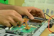
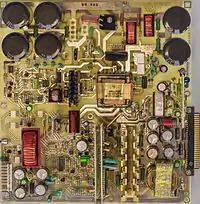
Reverse engineering of Printed circuit boards (sometimes called “cloning”, or PCB RE) is the process of generating fabrication and design data for an existing circuit board, either closely or exactly replicating its functionality.[1]

Obtaining circuit board design data is not by necessity malicious or aimed at intellectual property theft. The data generated in the reverse engineering process can be used for troubleshooting, repair, redesign and re-manufacturing, or even testing the security of a device to be used in a restricted environment.[2][3][4][5]
Uses
Legacy product support
Legacy systems need maintenance and replacement parts to operate past their intended life cycle. Demand for parts that are no longer being manufactured can lead to material shortages of parts, called DMS/DMSMS.
There is much demand that entire government divisions have been created to regulate and plan the obsolescence of those systems and parts. Areas commonly affected by technical obsolescence include power station controls, ATC and aviation controls, medical imaging systems, and many aspects of military technology.
There are many legacy systems developed in the 70s, 80s or 90s whose original manufacturer is no longer in business or no longer has the original design data, but whose original equipment is still in use. In many cases exact Form, fit and function is required, either that so parts can “handshake” properly with the existing framework, or to avoid requirements of time-consuming and costly testing.[1]
For industries with highly regulated electronics, (like military or aerospace) this approach can vastly reduce the time required to fabricate replacement parts for system repairs, since the new part's specifications match the original design exactly and therefore do not need to undergo the same level of rigorous re-certification and testing that would be required of a newly designed or revised circuit board.
For example, a power company in Florida was forced to shut down due to the failure of a single, inexpensive PCB, which had no replacement parts and no data available to print them. The failure occurred during peak usage hours, and a power outage at that time can cost a power company thousands of dollars per hour.[6]
An engineering firm successfully reverse engineered the PCB to generate an exact copy of the PCB using the destructive imaging and milling process, and the power station was subsequently able to resume normal operation.[7][8]
Benchmarking
The process can be used to provide important benchmarking information about newly acquired products, prototype PCBs or any circuit board the company does not own. For example, reverse engineering a circuit assembly reveals whether or not the fabricator has exactly matched the design specifications of the board.
The process can be used to inspect for counterfeit or malicious circuits embedded in a PCB, or, if a new product has been purchased by a company, to create schematics or other documentation that may not have been included with the product.[9][4]
Use with additive manufacturing
Data from the reverse engineering process can be used to immediately repair or reprint a circuit board using additive manufacturing techniques on multi-headed 3-D printers.
In situations where resources are limited like on a ship, submarine, space, or forward deployment, the reverse engineering process can enable a crew to maintain electronics equipment without being required to bring along spare parts. In an ideal scenario, the crew would have access to the design data to use with the 3D printer, but in the event that crew did not have the proper data for the PCBs, they would need to reverse engineer the artifact on hand to create more.[10]
Malicious Intent
Data from reverse engineering can be taken with good intentions but mitigating intellectual property theft and maintaining privacy is increasingly important. Obfuscating PCBs, or hiding the intent of processing is one way to help deter theft.[11] Another is using Physical Unclonable Functions (PUFs) as a digital fingerprint on your PCB that is impossible to recreate.[12]
Methods
Destructive RE
Destructive reverse engineering (DRE) is a process where all layers of the board are imaged and subsequently removed by various milling techniques or tools. While it is possible to use nearly any camera or image source for this method, purpose-built RE systems utilize calibrated image sources that allow for extremely accurate reproduction of the design data for the board. This allows an engineer to match the exact form, fit and function of the original PCB. The drawback to this method is that it destroys the PCB. If the data comes from the last remaining circuit card in existence, it cannot be compared to a sample since little or no circuit board remains at the end of the destructive process. Also, care must be taken during the milling process to avoid damaging the copper. If areas of copper are removed before they are imaged, this represents a permanent loss of data which can only be rectified by existing documentation of the PCB, or by reverse engineering a second, identical board.[9]
Non-Destructive RE


There is a growing desire and need for non-destructive reverse engineering technology (NDRE), especially in scenarios like the one mentioned above where there is only a single PCB that can be used. Non-destructive PCB RE (NDRE) mean that the circuit board itself is not destroyed in the process; however, most non-destructive techniques require removing components from the surface of the board.
The primary difference between DRE and NDRE methods are in the way that images for the board are captured before new data is generated - in some cases optical images of the top and bottom of the board are captured, then merged with X-ray images of the boards internal layers. Once all images of all of the layers of the board have been captured the process of generating digital manufacturing data is similar to the destructive process.[2][4]
X-ray Computed Tomography
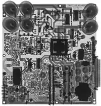
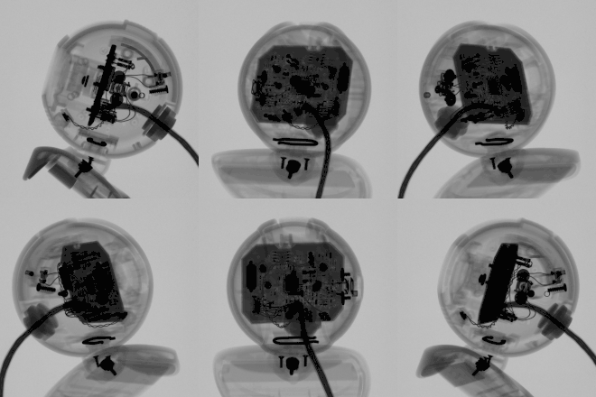
In recent years, X-ray computed tomography-based imaging processes have advanced to the point that they are able to capture images of the circuit board well enough to isolate individual layers and the features on each of these layers. For simpler boards, X-ray or CT Scans can provide high enough resolution images to reverse engineer a board without requiring the use of destructive milling.
Generally, a high resolution CT scanning machine will capture images of the board in 2-D slices, varying the angle and intensity. The resulting image captures of the board are computationally assembled into a 3-D volumetric model, and images of each layer can then be extracted. Additional research is underway presently to improve the procedure of CT scanning, volumetric data reconstruction, and circuit layer extraction.
In principle this process seems fairly simple, however certain issues such as the non-planarity of circuit layers, resolution and size limitations, and X-ray artifacting greatly complicate the extraction of usable circuit images.[4][13]
X-ray/CT imaging processes suffer many drawbacks, including resolution, equipment costs, and beam hardening and other X-ray artifacts which can distort images or make them harder to use for the reverse engineering process. Additionally, some IC chips can be damaged by exposure to powerful X-rays, so the board must be depopulated before being imaged if components are going to be salvaged for reuse.[4]
Another drawback is the time involved in creating the images used to generate circuit board design data. In one study, a Versa 510 X-ray machine was used to image a 6 layer board, measuring about 5 in × 8 in (130 mm × 200 mm) - the imaging and processing of the cloud data took over 18 hours to complete. By comparison, destructive reverse engineering can produce high resolution, calibrated optical images of the same 6 layer board in under 2 hours at very low cost by a skilled operator.[4]
Flying Probe Test
Oftentimes a Flying Probe test machine (FPT machine) can also be used to generate data from a circuit board. Unlike destructive methods, with this process the PCB can generally be reused. But the only output from this process is a list of connections between surface pads on the board, also known as a netlist.
The netlist is entirely dependent on the electrical connectivity of the PCB. If a PCB has become damaged or delaminated over the course of its life-cycle, it is possible that either via barrels or the copper traces have become broken, and if the damage occurs on the inner layers of the PCB, the FPT operator will have no way to know about the damage. The resulting netlist will reflect the breaks in the track, and should not be used to produce a schematic or additional boards. Additionally, a netlist is a fairly narrow data format that only provides insight into whether different component pins are connected or not. There is no information about the internal geometries of the copper circuits, which are crucial to proper functionality of radio emitting circuits, or circuits with differential signalling. It is impossible to create an identical PCB using this method. These drawbacks mean that this method is generally reserved for the creation of schematics or for troubleshooting and repair purposes.[9]
Films
Before the digital age of data processing and storage, PCB designers created and stored the designs on Mylar/BoPET drafting films, which were used in the photo-resistive fabrication process for circuit boards. These films were oftentimes the only copy of the design data for the board. While their primary use was in the manufacturing of PCBs they also doubled as their own storage media. Ultimately these films can disintegrate with time and use, so the design must be imaged and converted to vector formatting in order to be used for future fabrication. The reverse engineering of film sets is roughly the same process as reverse engineering a PCB - each layer is imaged, and Gerber/vector data is created for the different circuit layers.[1]
Final outputs and reproduction
Whether the board is reverse engineered using a destructive or non-destructive method, the result is that a netlist is obtained. While the netlist itself cannot be used to create an identical replacement, it can be used to generate supporting data for the board like a schematic. Whereas a netlist is a simple ASCII-based text file that simply lists all of the connections of the board, a PCB Schematic relays the same information in a more visual manner.
In addition, a schematic can be merged with the Bill of Materials (BOM) and component Pick and Place data to further enhance its usability in troubleshooting scenarios, or can be used as a base for the design of a brand new PCB. If a destructive RE process has been used or images for all PCB layers have been captured using X-ray imaging, the resulting data should include not only a netlist, BOM, and/or Schematic, but also a complete graphical layout of the copper layers of the board. This data can be represented in a vast number of different formats, but the most common data formats created in the reverse engineering process include the following:
- Circuit layers (Gerber RS274x, IPC-2581 or ODB++)
- Soldermask and solderpaste/stencil cut files (Gerber RS274x)
- Drill files (Excellon II/ASCII and/or Gerber RS274x)
- Plated and NonPlated Through-holes (Excellon II/ASCII)
- Per-layer Blind/Buried Drills (Excellon II/ASCII)
- Component Centroid/Pick-and-place data (ASCII) and component pinouts
- Component Netlist (IPC-D-356/ASCII)
- BOM (Spreadsheet)
- Schematics (PDF, Cadence Allegro, OrCAD, Altium, PADS, and other proprietary formats commonly available)[9][1]
The data produced in the reverse engineering process can be immediately sent to a PCB manufacturer for fabrication of replica/"clone" PCBs, or be used for creation of supporting documents.
References
- "Service Bureau". ScanCAD International. Retrieved 2020-03-30.
- Ng, Keng Tiong (28 February 2015). The art of PCB reverse engineering : unravelling the beauty of the original design. CreateSpace Independent Publishing Platform. ISBN 978-1-4993-2344-3. OCLC 950950597.
- Torrance, Randy; James, Dick (2009), The State-of-the-Art in IC Reverse Engineering, Lecture Notes in Computer Science, vol. 5747, Springer Berlin Heidelberg, pp. 363–381, doi:10.1007/978-3-642-04138-9_26, ISBN 978-3-642-04137-2
- Asadizanjani, Navid; Tehranipoor, Mark; Forte, Domenic (2017). "PCB Reverse Engineering Using Nondestructive X-ray Tomography and Advanced Image Processing". IEEE Transactions on Components, Packaging and Manufacturing Technology: 1–8. doi:10.1109/tcpmt.2016.2642824. ISSN 2156-3950. S2CID 9649818.
- "PCB". Retrieved 2023-03-07.
- "SAS Output". www.eia.gov. Retrieved 2020-03-31.
- "PCB Reverse Engineering". ScanCAD International. Retrieved 2020-03-31.
- "SAS Output". www.eia.gov. Retrieved 2020-03-31.
- PCB Reverse Engineering, retrieved 2020-03-31
- "nScrypt partners with ScanCAD International in Additive/FDM PCB manufacturing!". ScanCAD International. 2019-08-26. Retrieved 2020-03-31.
- Shakya, Bicky; Tehranipoor, Mark M.; Bhunia, Swarup; Forte, Domenic (2017), "Introduction to Hardware Obfuscation: Motivation, Methods and Evaluation", Hardware Protection through Obfuscation, Cham: Springer International Publishing, pp. 3–32, doi:10.1007/978-3-319-49019-9_1, ISBN 978-3-319-49018-2, retrieved 2023-04-07
- "Reliability assessment of integrated circuits through reverse engineering techniques". Microelectronics Reliability. 27 (3): 582. January 1987. doi:10.1016/0026-2714(87)90490-2. ISSN 0026-2714.
- Botero, Ulbert & Wilson, Ronald & Lu, Hangwei & Rahman, Mir & Mallaiyan, Mukhil & Ganji, Fatemeh & Asadizanjani, Navid & Tehranipoor, Mark & Woodard, Damon & Forte, Domenic. (2020). Hardware Trust and Assurance through Reverse Engineering: A Survey and Outlook from Image Analysis and Machine Learning Perspectives.
