Physical vapor deposition
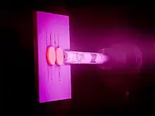
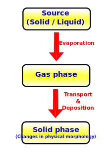
Physical vapor deposition (PVD), sometimes called physical vapor transport (PVT), describes a variety of vacuum deposition methods which can be used to produce thin films and coatings on substrates including metals, ceramics, glass, and polymers. PVD is characterized by a process in which the material transitions from a condensed phase to a vapor phase and then back to a thin film condensed phase. The most common PVD processes are sputtering and evaporation. PVD is used in the manufacturing of items which require thin films for optical, mechanical, electrical, acoustic or chemical functions. Examples include semiconductor devices such as thin-film solar cells,[1] microelectromechanical devices such as thin film bulk acoustic resonator, aluminized PET film for food packaging and balloons,[2] and titanium nitride coated cutting tools for metalworking. Besides PVD tools for fabrication, special smaller tools used mainly for scientific purposes have been developed.[3]


The source material is unavoidably also deposited on most other surfaces interior to the vacuum chamber, including the fixturing used to hold the parts. This is called overshoot.
Examples
- Cathodic arc deposition: a high-power electric arc discharged at the target (source) material blasts away some into highly ionized vapor to be deposited onto the workpiece.
- Electron-beam physical vapor deposition: the material to be deposited is heated to a high vapor pressure by electron bombardment in "high" vacuum and is transported by diffusion to be deposited by condensation on the (cooler) workpiece.
- Evaporative deposition: the material to be deposited is heated to a high vapor pressure by electrical resistance heating in "high" vacuum.[4][5]
- Close-space sublimation, the material, and substrate are placed close to one another and radiatively heated.
- Pulsed laser deposition: a high-power laser ablates material from the target into a vapor.
- Thermal laser epitaxy: a continuous-wave laser evaporates individual, free-standing elemental sources which then condense upon a substrate.
- Sputter deposition: a glow plasma discharge (usually localized around the "target" by a magnet) bombards the material sputtering some away as a vapor for subsequent deposition.
- Pulsed electron deposition: a highly energetic pulsed electron beam ablates material from the target generating a plasma stream under nonequilibrium conditions.
- Sublimation sandwich method: used for growing man-made crystals (silicon carbide, SiC).
Metrics and testing
Various thin film characterization techniques can be used to measure the physical properties of PVD coatings, such as:
- Calo tester: coating thickness test
- Nanoindentation: hardness test for thin-film coatings
- Pin-on-disc tester: wear and friction coefficient test
- Scratch tester: coating adhesion test
- X-ray micro-analyzer: investigation of structural features and heterogeneity of elemental composition for the growth surfaces [6]
Comparison to other deposition techniques
Advantages
- PVD coatings are sometimes harder and more corrosion-resistant than coatings applied by electroplating processes. Most coatings have high temperature and good impact strength, excellent abrasion resistance and are so durable that protective topcoats are rarely necessary.
- PVD coatings have the ability to utilize virtually any type of inorganic and some organic coating materials on an equally diverse group of substrates and surfaces using a wide variety of finishes.
- PVD process are often more environmentally friendly than traditional coating processes such as electroplating and painting.
- More than one technique can be used to deposit a given film.
Disadvantages
- Specific technologies can impose constraints; for example, the line-of-sight transfer is typical of most PVD coating techniques, however, some methods allow full coverage of complex geometries.
- Some PVD technologies operate at high temperatures and vacuums, requiring special attention by operating personnel and sometimes a cooling water system to dissipate large heat loads.
Applications
Anisotropic glasses
.jpg.webp)
PVD can be used as an application to make anisotropic glasses of low molecular weight for organic semiconductors.[7] The parameter needed to allow the formation of this type of glass is molecular mobility and anisotropic structure at the free surface of the glass.[7] The configuration of the polymer is important where it needs to be positioned in a lower energy state before the added molecules bury the material through a deposition. This process of adding molecules to the structure starts to equilibrate and gain mass and bulk out to have more kinetic stability.[7] The packing of molecules here through PVD is face-on, meaning not at the long tail end, allows further overlap of pi orbitals as well which also increases the stability of added molecules and the bonds. The orientation of these added materials is dependent mainly on temperature for when molecules will be deposited or extracted from the molecule.[7] The equilibration of the molecules is what provides the glass with its anisotropic characteristics. The anisotropy of these glasses is valuable as it allows a higher charge carrier mobility.[7] This process of packing in glass in an anisotropic way is valuable due to its versatility and the fact that glass provides added benefits beyond crystals, such as homogeneity and flexibility of composition.
Decorative applications
By varying the composition and duration of the process, a range of colors can be produced by PVD on stainless steel. The resulting colored stainless steel product can appear as brass, bronze, and other metals or alloys. This PVD-colored stainless steel can be used as exterior cladding for buildings and structures, such as the Vessel sculpture in New York City and The Bund in Shanghai. It is also used for interior hardware, paneling, and fixtures, and is even used on some consumer electronics, like the Space Gray and Gold finishes of the iPhone and Apple Watch.
Cutting tools
PVD is used to enhance the wear resistance of steel cutting tools' surfaces and decrease the risk of adhesion and sticking between tools and a workpiece. This includes tools used in metalworking or plastic injection molding.[8]: 2 The coating is typically a thin ceramic layer less than 4µm that has very high hardness and low friction. It is necessary to have high hardness of workpieces to ensure dimensional stability of coating to avoid brittling. It is possible to combine PVD with a plasma nitriding treatment of steel to increase the load bearing capacity of the coating.[8]: 2 Chromium nitride (CrN), titanium nitride (TiN), and Titanium Carbonitride (TiCN) may be used for PVD coating for plastic molding dies.[8]: 5
Other applications
PVD coatings are generally used to improve hardness, increase wear resistance, and prevent oxidation. They can also be used for aesthetic purposes. Thus, such coatings are used in a wide range of applications such as:
- Aerospace industry
- Architectural ironmongery, panels, and sheets
- Automotive industry
- Dyes and molds
- Firearms
- Optics
- Watches
- Jewelry
- Thin film applications (window tint, food packaging, etc.)
See also
- HPCVD – Thin-film deposition technique
- Chemical vapor deposition – Method used to apply surface coatings
- Ion plating – Method of coating solid surfaces with ions
- Thin-film deposition – Thin layer of material – Deposition of a thin layer of material
- Ion beam-assisted deposition – Materials engineering technique
References
- Selvakumar, N.; Barshilia, Harish C. (1 March 2012). "Review of physical vapor deposited (PVD) spectrally selective coatings for mid- and high-temperature solar thermal applications" (PDF). Solar Energy Materials and Solar Cells. 98: 1–23. doi:10.1016/j.solmat.2011.10.028.
- Hanlon, Joseph F.; Kelsey, Robert J.; Forcinio, Hallie (23 April 1998). "Chapter 4 Coatings and Laminations". Handbook of Package Engineering 3rd Edition. CRC Press. ISBN 978-1566763066.
- Fortunato, E.; Barquinha, P.; Martins, R. (12 June 2012). "Oxide Semiconductor Thin-Film Transistors: A Review of Recent Advances". Advanced Materials. 24 (22): 2945–2986. doi:10.1002/adma.201103228. ISSN 1521-4095. PMID 22573414. S2CID 205242464.
- He, Zhenping; Kretzschmar, Ilona (6 December 2013). "Template-Assisted GLAD: Approach to Single and Multipatch Patchy Particles with Controlled Patch Shape". Langmuir. 29 (51): 15755–15761. doi:10.1021/la404592z. PMID 24313824.
- He, Zhenping; Kretzschmar, Ilona (18 June 2012). "Template-Assisted Fabrication of Patchy Particles with Uniform Patches". Langmuir. 28 (26): 9915–9919. doi:10.1021/la3017563. PMID 22708736.
- Dunaev A.A., Egorova I.L. (2015). "Properties and optical application of polycrystalline zinc selenide obtained by physical vapor deposition". Scientific and Technical Journal of Information Technologies, Mechanics and Optics. 15 (3): 449–456. doi:10.17586/2226-1494-2015-15-3-449-456.
- Gujral, Ankit; Yu, Lian; Ediger, M.D. (1 April 2018). "Anisotropic organic glasses". Current Opinion in Solid State and Materials Science. 22 (2): 49–57. Bibcode:2018COSSM..22...49G. doi:10.1016/j.cossms.2017.11.001. ISSN 1359-0286. S2CID 102671908.
- "UDDEHOLM TOOL STEEL FOR PVD COATINGS" (PDF). 2020.
Further reading
- Anders, André, ed. (3 October 2000). Handbook of Plasma Immersion Ion Implantation and Deposition. Wiley-VCH. ISBN 978-0471246985.
- Bach, Hans; Krause, Dieter (10 July 2003). Thin Films on Glass. Springer. ISBN 978-3540585978.
- Bunshah, Roitan F (31 December 1994). Handbook of Deposition Technologies for Films and Coatings (Second ed.). William Andrew Publishing. ISBN 978-0815517467.
- Glaser, Hans Joachim (2000). Large Area Glass Coating. Von Ardenne Anlagentechnik GMBH. ISBN 978-3000049538.
- Glocker, D; Shah, S (17 December 2001). Handbook of Thin Film Process Technology. CRC Press. ISBN 978-0750308328.
- Mahan, John E (1 February 2000). Physical Vapor Deposition of Thin Films. Wiley-Interscience. ISBN 978-0471330011.
- Mattox, Donald M. (19 May 2010). Handbook of Physical Vapor Deposition (PVD) Processing (Second ed.). William Andrew Publishing. ISBN 978-0-815-52037-5.
- Mattox, Donald M (14 January 2004). The Foundations of Vacuum Coating Technology. William Andrew Publishing. ISBN 978-0815514954.
- Mattox, Donald M.; Mattox, Vivivenne Harwood (2007). 50 Years of Vacuum Coating Technology and the Growth of the Society of Vacuum Coaters. Society of Vacuum Coaters. ISBN 978-1878068279.
- Ohring, Milton (26 October 2001). Materials Science of Thin Films, Second Edition. Academic Press. ISBN 978-1493301720.
- Powell, Carroll F.; Oxley, Joseph H.; Blocher, John Milton (1966). Klerer, J. (ed.). "Vapor Deposition". Journal of the Electrochemical Society. The Electrochemical Society. 113 (10): 226–269. ASIN B007T4PDL6. Bibcode:1966JElS..113..266P. doi:10.1149/1.2423765.
- Snyder, Tim (6 May 2013). "What are PVD Wheels - Ask NASA". 4wheelonline.com. 4WheelOnline.com. Retrieved 3 October 2019.
- Westwood, William D (2003). Sputter Deposition - AVS Education Committee Book Series, Vol. 2. Education Committee, AVS. ISBN 978-0735401051.
- Willey, Ronald R (15 December 2007). Practical Monitoring and Control of Optical Thin Films. Willey Optical, Consultants. ISBN 978-0615181448.
- Willey, Ronald R (27 October 2007). Practical Equipment, Materials, and Processes for Optical Thin Films. Willey Optical, Consultants. ISBN 978-0615143972.
External links
- "Society of Vacuum Coaters". svc.org. Society of Vacuum Coaters. Retrieved 3 October 2019.
- Raghu, Saril (19 April 2009). Physical Vapor Desposition Tool. YouTube.com. Archived from the original on 19 December 2021. Retrieved 3 October 2019.