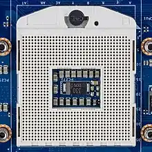
Socket G2
Socket G2, also known as rPGA 988B is Intel's CPU socket used with their line of mobile Core i7, the successor to the Core 2 line, and also with several mobile Core i5 and Core i3 processors. It is based on Intel's Sandy Bridge and Ivy Bridge architecture. Like its predecessor, socket G1 systems, it can only run in dual-channel memory mode, but with data rates up to 1600 MHz (as opposed to the triple-channel mode which is unique to the LGA-1366 platform and subsequent Xeon sockets). Socket G2 CPUs are also known as FCPGA988 socket processors, which should be pin compatible with PPGA988.[2]
 | |
| Type | rPGA |
|---|---|
| Contacts | 988 |
| FSB protocol | DMI |
| FSB frequency | 2.5 GT/s, 4.8 GT/s[1] |
| Voltage range | Max. 5 V with max. of 500 mA per pin |
| Processors |
|
| Predecessor | rPGA 988A (Socket G1) |
| Successor | rPGA 946B/947 (Socket G3) |
This article is part of the CPU socket series | |
Although nearly all motherboards using this socket are intended for mobile products like laptops, a few desktop boards using this do exist. Supermicro, for example, produced a number of mini ITX motherboards using the QM77 chipset.[3]
Technical specifications
- Pins arranged in a 35 × 36 grid array (it is incompatible with G1 socket due to different placing of one pin)
- 18 × 15 size grid removed from the center
- Utilization of cam-actuated retention mechanism
- The r in rPGA refers to reduced pitch which is 1 mm × 1 mm in this socket design.[4]
rPGA 989 (as shown on the right) is a socket that can take Socket G1 (rPGA988A) or Socket G2 (rPGA988B) processors.
Supported memory:
References
- Quoted from Intel's website and is reflected in the other reference links.
- "What is the difference between socket PPGA988 and FCPGA988?". Intel. Retrieved December 14, 2015.
- "3rd Generation Core™ Processor Based Motherboards". Supermicro. Retrieved January 6, 2015.
- "Molex Connector Part Number - 47989-0132". molex.com. Retrieved 2019-01-23.