Retinomorphic sensor
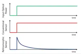
Retinomorphic sensors are a type of event-driven optical sensor which produce a signal in response to changes in light intensity, rather than to light intensity itself.[1] This is in contrast to conventional optical sensors such as charge coupled device (CCD) or complementary metal oxide semiconductor (CMOS) based sensors, which output a signal that increases with increasing light intensity. Because they respond to movement only, retinomorphic sensors are hoped to enable faster tracking of moving objects than conventional image sensors, and have potential applications in autonomous vehicles, robotics, and neuromorphic engineering.[2][3][4][5]

Naming and history
The first so-called artificial retina were reported in the late 1980's by Carver Mead and his doctoral students Misha Mahowald, and Tobias Delbrück.[6][7] These silicon-based sensors were based on small circuits involving differential amplifiers, capacitors, and resistors. The sensors produced a spike and subsequent decay in output voltage in response to a step-change in illumination intensity. This response is analogous to that of animal retinal cells, which in the 1920's were observed to fire more frequently when the intensity of light was changed than when it was constant.[8] The name silicon retina has hence been used to describe these sensors.[9]
The term retinomorphic was first used in a conference paper by Lex Akers in 1990.[10] The term received wider use by Stanford Professor of Engineering Kwabena Boahen, and has since been applied to a wide range of event-driven sensing strategies.[11] The word is analogous to neuromorphic, which is applied to hardware elements (such as processors) designed to replicate the way the brain processes information.
Operating principles

There are several retinomorphic sensor designs which yield a similar response. The first designs employed a differential amplifier which compared the input signal from of a conventional sensor (e.g. a phototransistor) to a filtered version of the output,[6] resulting in a gradual decay if the input was constant. Since the 1980's these sensors have evolved into much more complex and robust circuits.[1]
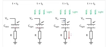
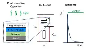
A more compact design of retinomorphic sensor consists of just a photosensitive capacitor and a resistor in series.[12] The output voltage of these retinomorphic sensors, , is defined as voltage dropped across the resistor. The photosensitive capacitor is designed to have a capacitance which is a function of incident light intensity. If a constant voltage , is applied across this RC circuit it will act as a passive high-pass filter and all voltage will be dropped across the capacitor (i.e. ). After a sufficient amount of time, the plates of the capacitor will be fully charged with a charge on each plate, where is the capacitance in the dark. Since under constant illumination, this can be simplified to .
If light is then applied to the capacitor it will change capacitance to a new value: . The charge that the plates can accommodate will therefore change to , leaving a surplus / deficit of charge on each plate. The excess charge will be forced to leave the plates, flowing either to ground or the input voltage terminal. The rate of charge flow is determined by the resistance of the resistor , and the capacitance of the capacitor. This charge flow will lead to a non-zero voltage being dropped across the resistor and hence a non-zero . After the charge stops flowing the system returns to steady-state, all the voltage is once again dropped across the capacitor, and again.

For a capacitor to change its capacitance under illumination, the dielectric constant of the insulator between the plates,[13] or the effective dimensions of the capacitor, must be illumination-dependent. The effective dimensions can be changed by using a bilayer material between the plates, consisting of an insulator and a semiconductor. Under appropriate illumination conditions the semiconductor will increase its conductivity when exposed to light, emulating the process of moving the plates of the capacitor closer together, and therefore increasing capacitance. For this to be possible, the semiconductor must have a low electrical conductivity in the dark, and have an appropriate band gap to enable charge generation under illumination. The device must also allow optical access to the semiconductor, through a transparent plate (e.g. using a transparent conducting oxide).
Applications
Conventional cameras capture every part of an image, regardless of whether it is relevant to the task. Because every pixel is measured, conventional image sensors are only able to sample the visual field at relatively low frame rates, typically 30 - 240 frames per second. Even in professional high speed cameras used for motion picture, the frame rate is limited to a few 10's of thousands of frames per second for a full resolution image. This limitation could represent a performance bottleneck in the identification of high speed moving objects. This is particularly critical in applications where rapid identification of movement is critical, such as in autonomous vehicles.
By contrast, retinomorphic sensors identify movement by design. This means that they do not have a frame rate and instead are event-driven, responding only when needed. For this reason, retinomorphic sensors are hoped to enable identification of moving objects much more quickly than conventional real-time image analysis strategies.[4] Retinomorphic sensors are therefore hoped to have applications in autonomous vehicles,[14][15] robotics,[16] and neuromorphic engineering.[17]
Theory
Retinomorphic sensor operation can be quantified using similar techniques to simple RC circuits, the only difference being that capacitance is not constant as a function of time in a retinomorphic sensor.[18] If the input voltage is defined as , the voltage dropped across the resistor as , and the voltage dropped across the capacitor as , we can use Kirchhoff's Voltage Law to state:
Defining the current flowing through the resistor as , we can use Ohm's Law to write:
From the definition of current, we can then write this in terms of charge, , flowing off the bottom plate:
where is time. Charge on the capacitor plates is defined by the product of capacitance, , and the voltage across the capacitor, , we can hence say:
Because capacitance in retinomorphic sensors is a function of time, cannot be taken out of the derivative as a constant. Using the product rule, we get the following general equation of retinomorphic sensor response:
or, in terms of the output voltage:
Response to a step-change in intensity
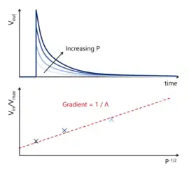
While the equation above is valid for any form of , it cannot be solved analytically unless the input form of the optical stimulus is known. The simplest form of optical stimulus would be a step function going from zero to some finite optical power density at a time . While real-world applications of retinomorphic sensors are unlikely to be accurately described by such events, it is a useful way to understand and benchmark the performance of retinomorphic sensors. In particular, we are primarily concerned with the maximum height of the immediately after the light has been turned on.
In this case the capacitance could be described by:
The capacitance under illumination will depend on . Semiconductors are known[19] to have a conductance, , which increases with a power-law dependence on incident optical power density: , where is a dimensionless exponent. Since is linearly proportional to charge density, and capacitance is linearly proportional to charges on the plates for a given voltage, the capacitance of a retinomorphic sensor also has a power-law dependence on . The capacitance as a function of time in response to a step function, can therefore be written as:
where is the capacitance prefactor. For a step function we can re-write our differential equation for as a difference equation:
where is the change in voltage dropped across the capacitor as a result of turning on the light, is the change in capacitance as a result of turning on the light, and is the time taken for the light to turn on. The variables and are defined as the voltage dropped across the capacitor and the capacitance, respectively, immediately after the light has been turned on. I.e. is henceforth shorthand for , and is henceforth shorthand for . Assuming the sensor has been held in the dark for sufficiently long before the light is turned on, the change in can hence be written as:
Similarly, the change in can be written as
Putting these into the difference equation for :

Multiplying this out:
Since we are assuming the light turns on very quickly we can approximate . This leads to the following:
Using the relationship , this can then be written in terms of the output voltage:
Where we have defined the peak height as , since he peak occurs immediately after the light has been turned on.
The retinomorphic figure of merit, , is defined as the ratio of the capacitance prefactor and the capacitance of the retinomorphic sensor in the dark:[18]
With this parameter, the inverse ratio of peak height to input voltage can be written as follows:
The value of will depend on the nature of recombination in the semiconductor,[20] but if band-to-band recombination dominates and the charge density of electrons and holes are equal, . For systems where this is approximately true[21] the following simplification to the above equation an be made:
This equation provides a simple method for evaluating the retinomorphic figure of merit from experimental data. This can be carried out by measuring the peak height, , of a retinomorphic sensor in response to a step change in light intensity from 0 to , for a range of values . Plotting as a function of should yield a straight line with a gradient of . This approach assumes that is linearly proportional to .
See also
References
- Posch, Christoph; Serrano-Gotarredona, Teresa; Linares-Barranco, Bernabe; Delbruck, Tobi (2014). "Retinomorphic Event-Based Vision Sensors: Bioinspired Cameras With Spiking Output". Proceedings of the IEEE. 102 (10): 1470–1484. doi:10.1109/JPROC.2014.2346153. hdl:11441/102353. ISSN 1558-2256. S2CID 11513955.
- Mahowald, Misha A.; Mead, Carver (1991). "The Silicon Retina". Scientific American. 264 (5): 76–82. Bibcode:1991SciAm.264e..76M. doi:10.1038/scientificamerican0591-76. PMID 2052936. Retrieved 2021-12-28.
- Gilder, George F. (2005). The Silicon Eye. W. W. Norton & Company. ISBN 978-0-393-05763-8.
- Hambling, David. "AI vision could be improved with sensors that mimic human eyes". New Scientist. Retrieved 2021-10-28.
- "An eye for an AI: Optic device mimics human retina". BBC Science Focus Magazine. Retrieved 2021-10-28.
- Delbrück, T.; Mead, C. A. (1989), Touretzky, D. S. (ed.), An Electronic Photoreceptor Sensitive to Small Changes in Intensity, vol. 1, San Mateo, CA: Morgan Kaufmann Publishers, pp. 720–727, ISBN 978-1-55860-015-7, retrieved 2021-12-23
- Mead, Carver A.; Mahowald, M. A. (1988-01-01). "A silicon model of early visual processing". Neural Networks. 1 (1): 91–97. doi:10.1016/0893-6080(88)90024-X. ISSN 0893-6080.
- Adrian, E. D.; Matthews, Rachel (1927). "The action of light on the eye". The Journal of Physiology. 63 (4): 378–414. doi:10.1113/jphysiol.1927.sp002410. ISSN 1469-7793. PMC 1514941. PMID 16993896.
- Delbruck, T. (1993). "Silicon retina with correlation-based, velocity-tuned pixels". IEEE Transactions on Neural Networks. 4 (3): 529–541. doi:10.1109/72.217194. ISSN 1941-0093. PMID 18267755.
- Rao, A.; Akers, L.A. (1990). "A retinomorphic VLSI smart sensor for invariant geometric object recognition". 1990 IJCNN International Joint Conference on Neural Networks. pp. 949–954 vol.2. doi:10.1109/IJCNN.1990.137961. S2CID 35554142.
- Boahen, K. (1996). "Retinomorphic vision systems". Proceedings of Fifth International Conference on Microelectronics for Neural Networks. pp. 2–14. doi:10.1109/MNNFS.1996.493766. ISBN 0-8186-7373-7. S2CID 62609792.
- Trujillo Herrera, Cinthya; Labram, John G. (2020-12-07). "A perovskite retinomorphic sensor". Applied Physics Letters. 117 (23): 233501. Bibcode:2020ApPhL.117w3501T. doi:10.1063/5.0030097. ISSN 0003-6951. S2CID 230546095.
- Dillman, Norman (1965). "Photodielectric effect in semiconductors". PhD Thesis.
- IOM3. "Optical sensor mimics human eye for self-driving cars". www.iom3.org. Retrieved 2021-12-29.
- "Simple Eyelike Sensors Could Make AI Systems More Efficient". Inside Science. 8 December 2020. Retrieved 2021-12-29.
- "Bigger boost in robot's field of view". ZME Science. 2021-01-05. Retrieved 2021-12-29.
- "Perovskite sensor sees more like the human eye". Physics World. 2021-01-18. Retrieved 2021-12-29.
- Trujillo Herrera, Cinthya; Labram, John G (2021-09-16). "Quantifying the performance of perovskite retinomorphic sensors". Journal of Physics D: Applied Physics. 54 (47): 475110. doi:10.1088/1361-6463/ac1d10. ISSN 0022-3727. S2CID 237541793.
- "Photoelectronic Properties of Semiconductors | Materials science". Cambridge University Press. Retrieved 2021-12-28.
- Balberg, I. (1994-01-15). "The two carriers' mobility‐lifetime products and their light intensity dependencies in hydrogenated amorphous silicon". Journal of Applied Physics. 75 (2): 914–923. Bibcode:1994JAP....75..914B. doi:10.1063/1.356447. ISSN 0021-8979.
- Levine, Igal; Gupta, Satyajit; Brenner, Thomas M.; Azulay, Doron; Millo, Oded; Hodes, Gary; Cahen, David; Balberg, Isaac (2016-12-15). "Mobility–Lifetime Products in MAPbI3 Films". The Journal of Physical Chemistry Letters. 7 (24): 5219–5226. doi:10.1021/acs.jpclett.6b02287. PMID 27973905.