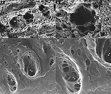
Scanning helium ion microscope
A scanning helium ion microscope (SHIM, HeIM or HIM) is an imaging technology based on a scanning helium ion beam.[2] Similar to other focused ion beam techniques, it allows to combine milling and cutting of samples with their observation at sub-nanometer resolution.[3]
.jpg.webp)

In terms of imaging, SHIM has several advantages over the traditional scanning electron microscope (SEM). Owing to the very high source brightness, and the short De Broglie wavelength of the helium ions, which is inversely proportional to their momentum, it is possible to obtain qualitative data not achievable with conventional microscopes which use photons or electrons as the emitting source. As the helium ion beam interacts with the sample, it does not suffer from a large excitation volume, and hence provides sharp images with a large depth of field on a wide range of materials. Compared to a SEM, the secondary electron yield is quite high, allowing for imaging with currents as low as 1 femtoamp. The detectors provide information-rich images which offer topographic, material, crystallographic, and electrical properties of the sample. In contrast to other ion beams, there is no discernible sample damage due to relatively light mass of the helium ion. The drawback is the cost.
SHIMs have been commercially available since 2007,[4] and a surface resolution of 0.24 nanometers has been demonstrated.[5][6]
References
- Bidlack, Felicitas B.; Huynh, Chuong; Marshman, Jeffrey; Goetze, Bernhard (2014). "Helium ion microscopy of enamel crystallites and extracellular tooth enamel matrix". Frontiers in Physiology. 5: 395. doi:10.3389/fphys.2014.00395. PMC 4193210. PMID 25346697.
- NanoTechWire.com Press Release: ALIS Corporation Announces Breakthrough in Helium Ion Technology for Next-Generation Atomic-Level Microscope, December 7, 2005 (retrieved on November 22, 2008)
- Iberi, Vighter; Vlassiouk, Ivan; Zhang, X.-G.; Matola, Brad; Linn, Allison; Joy, David C.; Rondinone, Adam J. (2015). "Maskless Lithography and in situ Visualization of Conductivity of Graphene using Helium Ion Microscopy". Scientific Reports. 5: 11952. Bibcode:2015NatSR...511952I. doi:10.1038/srep11952. PMC 4493665. PMID 26150202.
- Carl Zeiss SMT Press Release: Carl Zeiss SMT Ships World’s First ORION Helium Ion Microscope to U.S. National Institute of Standards and Technology Archived July 18, 2011, at archive.today, July 17, 2008 (retrieved on November 22, 2008)
- Fabtech.org: Microscopy resolution record claimed by Carl Zeiss, November 21, 2008 (retrieved on November 22, 2008)
- Carl Zeiss SMT Press Release: Carl Zeiss Sets New World Record in Microscopy Resolution Using Scanning Helium Ions Archived May 1, 2009, at the Wayback Machine, November 21, 2008 (retrieved on November 22, 2008)
External links
- Carl Zeiss SMT – Nano Technology Systems Division: ORION He-Ion microscope
- Microscopy Today, Volume 14, Number 04, July 2006: An Introduction to the Helium Ion Microscope
- How New Helium Ion Microscope Measures Up – ScienceDaily