Stranski–Krastanov growth
Stranski–Krastanov growth (SK growth, also Stransky–Krastanov or 'Stranski–Krastanow') is one of the three primary modes by which thin films grow epitaxially at a crystal surface or interface. Also known as 'layer-plus-island growth', the SK mode follows a two step process: initially, complete films of adsorbates, up to several monolayers thick, grow in a layer-by-layer fashion on a crystal substrate. Beyond a critical layer thickness, which depends on strain and the chemical potential of the deposited film, growth continues through the nucleation and coalescence of adsorbate 'islands'.[1][2][3][4] This growth mechanism was first noted by Ivan Stranski and Lyubomir Krastanov in 1938.[5] It wasn't until 1958 however, in a seminal work by Ernst Bauer published in Zeitschrift für Kristallographie, that the SK, Volmer–Weber, and Frank–van der Merwe mechanisms were systematically classified as the primary thin-film growth processes.[6] Since then, SK growth has been the subject of intense investigation, not only to better understand the complex thermodynamics and kinetics at the core of thin-film formation, but also as a route to fabricating novel nanostructures for application in the microelectronics industry.
Modes of thin-film growth

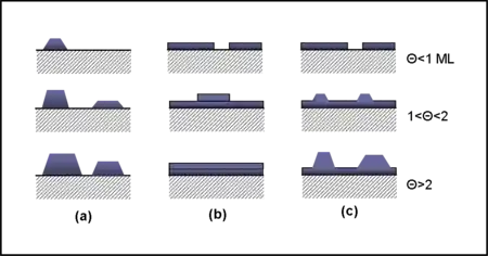
The growth of epitaxial (homogeneous or heterogeneous) thin films on a single crystal surface depends critically on the interaction strength between adatoms and the surface. While it is possible to grow epilayers from a liquid solution, most epitaxial growth occurs via a vapor phase technique such as molecular beam epitaxy (MBE). In Volmer–Weber (VW) growth, adatom–adatom interactions are stronger than those of the adatom with the surface, leading to the formation of three-dimensional adatom clusters or islands.[3] Growth of these clusters, along with coarsening, will cause rough multi-layer films to grow on the substrate surface. Antithetically, during Frank–van der Merwe (FM) growth, adatoms attach preferentially to surface sites resulting in atomically smooth, fully formed layers. This layer-by-layer growth is two-dimensional, indicating that complete films form prior to growth of subsequent layers.[2][3] Stranski–Krastanov growth is an intermediary process characterized by both 2D layer and 3D island growth. Transition from the layer-by-layer to island-based growth occurs at a critical layer thickness which is highly dependent on the chemical and physical properties, such as surface energies and lattice parameters, of the substrate and film.[1][2][3] Figure 1 is a schematic representation of the three main growth modes for various surface coverages.
Determining the mechanism by which a thin film grows requires consideration of the chemical potentials of the first few deposited layers.[2][7] A model for the layer chemical potential per atom has been proposed by Markov as:[7]
where is the bulk chemical potential of the adsorbate material, is the desorption energy of an adsorbate atom from a wetting layer of the same material, the desorption energy of an adsorbate atom from the substrate, is the per atom misfit dislocation energy, and the per atom homogeneous strain energy. In general, the values of , , , and depend in a complex way on the thickness of the growing layers and lattice misfit between the substrate and adsorbate film. In the limit of small strains, , the criterion for a film growth mode is dependent on .
- VW growth: (adatom cohesive force is stronger than surface adhesive force)
- FM growth: (surface adhesive force is stronger than adatom cohesive force)
SK growth can be described by both of these inequalities. While initial film growth follows an FM mechanism, i.e. positive differential μ, nontrivial amounts of strain energy accumulate in the deposited layers. At a critical thickness, this strain induces a sign reversal in the chemical potential, i.e. negative differential μ, leading to a switch in the growth mode. At this point it is energetically favorable to nucleate islands and further growth occurs by a VW type mechanism.[7] A thermodynamic criterion for layer growth similar to the one presented above can be obtained using a force balance of surface tensions and contact angle.[8]


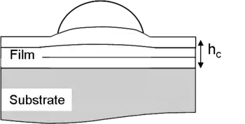
Since the formation of wetting layers occurs in a commensurate fashion at a crystal surface, there is often an associated misfit between the film and the substrate due to the different lattice parameters of each material. Attachment of the thinner film to the thicker substrate induces a misfit strain at the interface given by . Here and are the film and substrate lattice constants, respectively. As the wetting layer thickens, the associated strain energy increases rapidly. In order to relieve the strain, island formation can occur in either a dislocated or coherent fashion. In dislocated islands, strain relief arises by forming interfacial misfit dislocations. The reduction in strain energy accommodated by introducing a dislocation is generally greater than the concomitant cost of increased surface energy associated with creating the clusters. The thickness of the wetting layer at which island nucleation initiates, called the critical thickness , is strongly dependent on the lattice mismatch between the film and substrate, with a greater mismatch leading to smaller critical thicknesses.[9] Values of can range from submonlayer coverage to up to several monolayers thick.[1][10] Figure 2 illustrates a dislocated island during SK growth after reaching a critical layer height. A pure edge dislocation is shown at the island interface to illustrate the relieved structure of the cluster.
In some cases, most notably the Si/Ge system, nanoscale dislocation-free islands can be formed during SK growth by introducing undulations into the near surface layers of the substrate.[11][12][13][14][10] These regions of local curvature serve to elastically deform both the substrate and island, relieving accumulated strain and bringing the wetting layer and island lattice constant closer to its bulk value. This elastic instability at is known as the Grinfeld instability (formerly Asaro–Tiller–Grinfeld; ATG).[7] The resulting islands are coherent and defect-free, garnering them significant interest for use in nanoscale electronic and optoelectronic devices. Such applications are discussed briefly later. A schematic of the resulting epitaxial structure is shown in figure 3 which highlights the induced radius of curvature at the substrate surface and in the island. Finally, strain stabilization indicative of coherent SK growth decreases with decreasing inter-island separation. At large areal island densities (smaller spacing), curvature effects from neighboring clusters will cause dislocation loops to form leading to defected island creation.[11]
Monitoring SK growth
Wide beam techniques

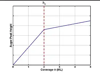
Analytical techniques such as Auger electron spectroscopy (AES), low-energy electron diffraction (LEED), and reflection high energy electron diffraction (RHEED), have been extensively used to monitor SK growth. AES data obtained in situ during film growth in a number model systems, such as Pd/W(100), Pb/Cu(110), Ag/W(110), and Ag/Fe(110), show characteristic segmented curves like those presented in figure 4.[1][2][11] Height of the film Auger peaks plotted as a function of surface coverage Θ, initially exhibits a straight line, which is indicative of AES data for FM growth. There is a clear break point at a critical adsorbate surface coverage followed by another linear segment at a reduced slope. The paired break point and shallow line slope is characteristic of island nucleation; a similar plot for FM growth would exhibit many such line and break pairs while a plot of the VW mode would be a single line of low slope. In some systems, reorganization of the 2D wetting layer results in decreasing AES peaks with increasing adsorbate coverage.[11] Such situations arise when many adatoms are required to reach a critical nucleus size on the surface and at nucleation the resulting adsorbed layer constitutes a significant fraction of a monolayer. After nucleation, metastable adatoms on the surface are incorporated into the nuclei, causing the Auger signal to fall. This phenomenon is particularly evident for deposits on a molybdenum substrate.
Evolution of island formation during a SK transitions have also been successfully measured using LEED and RHEED techniques. Diffraction data obtained via various LEED experiments have been effectively used in conjunction with AES to measure the critical layer thickness at the onset of island formation.[2][11] In addition, RHEED oscillations have proven very sensitive to the layer-to-island transition during SK growth, with the diffraction data providing detailed crystallographic information about the nucleated islands. Following the time dependence of LEED, RHEED, and AES signals, extensive information on surface kinetics and thermodynamics has been gathered for a number of technologically relevant systems.
Microscopies
Unlike the techniques presented in the last section in which probe size can be relatively large compared to island size, surface microscopies such scanning electron microscopy (SEM), transmission electron microscopy (TEM), scanning tunneling microscopy (STM), and Atomic force microscopy (AFM) offer the opportunity for direct viewing of deposit/substrate combination events.[1][3][11] The extreme magnifications afforded by these techniques, often down to the nanometer length scale, make them particularly applicable for visualizing the strongly 3D islands. UHV-SEM and TEM are routinely used to image island formation during SK growth, enabling a wide range of information to be gathered, ranging from island densities to equilibrium shapes.[1][2][3] AFM and STM have become increasingly utilized to correlate island geometry to the surface morphology of the surrounding substrate and wetting layer.[14] These visualization tools are often used to complement quantitative information gathered during wide-beam analyses.
Application to nanotechnology
As mentioned previously, coherent island formation during SK growth has attracted increased interest as a means for fabricating epitaxial nanoscale structures, particularly quantum dots (QDs).[12][13][14][15][16] Widely used quantum dots grown in the SK-growth-mode are based on the material combinations Si/Ge or InAs/GaAs.[17] Significant effort has been spent developing methods to control island organization, density, and size on a substrate. Techniques such as surface dimpling with a pulsed laser and control over growth rate have been successfully applied to alter the onset of the SK transition or even suppress it altogether.[14][18] The ability to control this transition either spatially or temporally enables manipulation of physical parameters of the nanostructures, like geometry and size, which, in turn, can alter their electronic or optoelectronic properties (i.e. band gap). For example, Schwarz–Selinger, et al. have used surface dimpling to create surface miscuts on Si that provide preferential Ge island nucleation sites surrounded by a denuded zone.[14] In a similar fashion, lithographically patterned substrates have been used as nucleation templates for SiGe clusters.[13][15] Several studies have also shown that island geometries can be altered during SK growth by controlling substrate relief and growth rate.[14][16] Bimodal size distributions of Ge islands on Si are a striking example of this phenomenon in which pyramidal and dome-shaped islands coexist after Ge growth on a textured Si substrate.[14] Such ability to control the size, location, and shape of these structures could provide invaluable techniques for 'bottom-up' fabrication schemes of next-generation devices in the microelectronics industry.
See also
References
- Venables, John (2000). Introduction to Surface and Thin Film Processes. Cambridge: Cambridge University Press. ISBN 0-521-62460-6.
- Pimpinelli, Alberto; Jacques Villain (1998). Physics of Crystal Growth. Cambridge: Cambridge University Press. ISBN 0-521-55198-6.
- Oura, K.; V.G. Lifshits; A.A. Saranin; A.V. Zotov; M. Katayama (2003). Surface Science: An Introduction. Berlin: Springer. ISBN 3-540-00545-5.
- Eaglesham, D.J.; M. Cerullo (April 1990). "Dislocation-free Stranski-Krastanow growth of Ge on Si(100)". Physical Review Letters. 64 (16): 1943–1946. Bibcode:1990PhRvL..64.1943E. doi:10.1103/PhysRevLett.64.1943. PMID 10041534.
- Stranski, Ivan N.; Krastanow, Lubomir (1938). "Zur Theorie der orientierten Ausscheidung von Ionenkristallen aufeinander". Abhandlungen der Mathematisch-Naturwissenschaftlichen Klasse IIb. Akademie der Wissenschaften Wien. 146: 797–810.
- Bauer, Ernst (1958). "Phänomenologische Theorie der Kristallabscheidung an Oberflächen. I". Zeitschrift für Kristallographie. 110 (1–6): 372–394. Bibcode:1958ZK....110..372B. doi:10.1524/zkri.1958.110.1-6.372.
- Markov, Ivan V. (1995). Crystal Growth for Beginners: Fundamentals of Nucleation, Crystal Growth, and Epitaxy. Singapore: World Scientific. ISBN 981-02-1531-2.
- See for example Oura et al (Surface Science) or Venables (Introduction to Surface and Thin Film Processes).
- Matthews, John Wauchope (1975). Epitaxial Growth. New York: Academic Press. ISBN 0-12-480901-4.
- Kukta, R.V.; L.B. Freund (November–December 1997). "Minimum energy configuration of epitaxial material clusters on a lattice-mismatched substrate". Journal of the Mechanics and Physics of Solids. 45 (11–12): 1835–1860. Bibcode:1997JMPSo..45.1835K. doi:10.1016/S0022-5096(97)00031-8.
- Venables, John; G. D. T. Spiller; M. Hanbucken (April 1984). "Nucleation and growth of thin films". Reports on Progress in Physics. 47 (4): 399–459. Bibcode:1984RPPh...47..399V. doi:10.1088/0034-4885/47/4/002. S2CID 250916067.
- Li, Y.R.; Z. Liang; Y. Zhang; J. Zhu; S.W. Jiang; X.H. Wei (October 2005). "Growth modes transition induced by strain relaxation in epitaxial MgO thin films on SrTiO3 (001) substrates". Thin Solid Films. 489 (1–2): 245–250. Bibcode:2005TSF...489..245L. doi:10.1016/j.tsf.2005.04.095.
- Chiu, C.-h.; Z. Huang; C. T. Poh (September 2004). "Formation of Nanostructures by the Activated Stranski-Krastanow Transition Method". Physical Review Letters. 93 (13): 36105. Bibcode:2004PhRvL..93m6105C. doi:10.1103/PhysRevLett.93.136105. PMID 15524741.
- Schwarz-Selinger, T.; Y. L. Foo; David G. Cahill; J. E. Greene (March 2002). "Surface mass transport and island nucleation during growth of Ge on laser textured Si(001)". Physical Review B. 53 (12): 125317. Bibcode:2002PhRvB..65l5317S. doi:10.1103/PhysRevB.65.125317.
- Bauer, G.; F. Schäffler (November 2006). "Self-assembled Si and SiGe nanostructures: New growth concepts and structural analysis Physica Status Solidi A". Physica Status Solidi. 203 (14): 3496–3505. Bibcode:2006PSSAR.203.3496B. doi:10.1002/pssa.200622405. S2CID 123594884.
- Shklyaev, O.E.; M. J. Beck; M. Asta; M. J. Miksis; P. W. Voorhees (May 2005). "Role of Strain-Dependent Surface Energies in Ge/Si(100) Island Formation". Physical Review Letters. 94 (17): 176102. Bibcode:2005PhRvL..94q6102S. doi:10.1103/PhysRevLett.94.176102. PMID 15904314.
- Leonard, D.; Pond, K.; Petroff, P. M. (1994). "Critical layer thickness for self-assembled InAs islands on GaAs". Physical Review B. 50 (16): 11687–11692. Bibcode:1994PhRvB..5011687L. doi:10.1103/PhysRevB.50.11687. ISSN 0163-1829. PMID 9975303.
- Watanabe, Fumiya; David G. Cahill; J. E. Greene (February 2005). "Roughening Rates of Strained-Layer Instabilities". Physical Review Letters. 94 (6): 066101. Bibcode:2005PhRvL..94f6101W. doi:10.1103/PhysRevLett.94.066101. PMID 15783751.