Superlattice
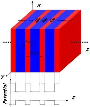
A superlattice is a periodic structure of layers of two (or more) materials. Typically, the thickness of one layer is several nanometers. It can also refer to a lower-dimensional structure such as an array of quantum dots or quantum wells.
Discovery
Superlattices were discovered early in 1925 by Johansson and Linde[1] after the studies on gold-copper and palladium-copper systems through their special X-ray diffraction patterns. Further experimental observations and theoretical modifications on the field were done by Bradley and Jay,[2] Gorsky,[3] Borelius,[4] Dehlinger and Graf,[5] Bragg and Williams[6] and Bethe.[7] Theories were based on the transition of arrangement of atoms in crystal lattices from disordered state to an ordered state.
Mechanical properties
J.S. Koehler theoretically predicted[8] that by using alternate (nano-)layers of materials with high and low elastic constants, shearing resistance is improved by up to 100 times as the Frank–Read source of dislocations cannot operate in the nanolayers.
The increased mechanical hardness of such superlattice materials was confirmed firstly by Lehoczky in 1978 on Al-Cu and Al-Ag,[9] and later on by several others, such as Barnett and Sproul[10] on hard PVD coatings.
Semiconductor properties
If the superlattice is made of two semiconductor materials with different band gaps, each quantum well sets up new selection rules that affect the conditions for charges to flow through the structure. The two different semiconductor materials are deposited alternately on each other to form a periodic structure in the growth direction. Since the 1970 proposal of synthetic superlattices by Esaki and Tsu,[11] advances in the physics of such ultra-fine semiconductors, presently called quantum structures, have been made. The concept of quantum confinement has led to the observation of quantum size effects in isolated quantum well heterostructures and is closely related to superlattices through the tunneling phenomena. Therefore, these two ideas are often discussed on the same physical basis, but each has different physics useful for applications in electric and optical devices.
Semiconductor superlattice types
Superlattice miniband structures depend on the heterostructure type, either type I, type II or type III. For type I the bottom of the conduction band and the top of the valence subband are formed in the same semiconductor layer. In type II the conduction and valence subbands are staggered in both real and reciprocal space, so that electrons and holes are confined in different layers. Type III superlattices involve semimetal material, such as HgTe/CdTe. Although the bottom of the conduction subband and the top of the valence subband are formed in the same semiconductor layer in Type III superlattice, which is similar with Type I superlattice, the band gap of Type III superlattices can be continuously adjusted from semiconductor to zero band gap material and to semimetal with negative band gap.
Another class of quasiperiodic superlattices is named after Fibonacci. A Fibonacci superlattice can be viewed as a one-dimensional quasicrystal, where either electron hopping transfer or on-site energy takes two values arranged in a Fibonacci sequence.
Semiconductor materials

Semiconductor materials, which are used to fabricate the superlattice structures, may be divided by the element groups, IV, III-V and II-VI. While group III-V semiconductors (especially GaAs/AlxGa1−xAs) have been extensively studied, group IV heterostructures such as the SixGe1−x system are much more difficult to realize because of the large lattice mismatch. Nevertheless, the strain modification of the subband structures is interesting in these quantum structures and has attracted much attention.
In the GaAs/AlAs system both the difference in lattice constant between GaAs and AlAs and the difference of their thermal expansion coefficient are small. Thus, the remaining strain at room temperature can be minimized after cooling from epitaxial growth temperatures. The first compositional superlattice was realized using the GaAs/AlxGa1−xAs material system.
A graphene/boron nitride system forms a semiconductor superlattice once the two crystals are aligned. Its charge carriers move perpendicular to the electric field, with little energy dissipation. h-BN has a hexagonal structure similar to graphene's. The superlattice has broken inversion symmetry. Locally, topological currents are comparable in strength to the applied current, indicating large valley-Hall angles.[12]
Production
Superlattices can be produced using various techniques, but the most common are molecular-beam epitaxy (MBE) and sputtering. With these methods, layers can be produced with thicknesses of only a few atomic spacings. An example of specifying a superlattice is [Fe
20V
30]20. It describes a bi-layer of 20Å of Iron (Fe) and 30Å of Vanadium (V) repeated 20 times, thus yielding a total thickness of 1000Å or 100 nm. The MBE technology as a means of fabricating semiconductor superlattices is of primary importance. In addition to the MBE technology, metal-organic chemical vapor deposition (MO-CVD) has contributed to the development of superconductor superlattices, which are composed of quaternary III-V compound semiconductors like InGaAsP alloys. Newer techniques include a combination of gas source handling with ultrahigh vacuum (UHV) technologies such as metal-organic molecules as source materials and gas-source MBE using hybrid gases such as arsine (AsH
3) and phosphine (PH
3) have been developed.
Generally speaking MBE is a method of using three temperatures in binary systems, e.g., the substrate temperature, the source material temperature of the group III and the group V elements in the case of III-V compounds.
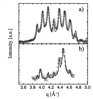
The structural quality of the produced superlattices can be verified by means of X-ray diffraction or neutron diffraction spectra which contain characteristic satellite peaks. Other effects associated with the alternating layering are: giant magnetoresistance, tunable reflectivity for X-ray and neutron mirrors, neutron spin polarization, and changes in elastic and acoustic properties. Depending on the nature of its components, a superlattice may be called magnetic, optical or semiconducting.

Miniband structure
The schematic structure of a periodic superlattice is shown below, where A and B are two semiconductor materials of respective layer thickness a and b (period: ). When a and b are not too small compared with the interatomic spacing, an adequate approximation is obtained by replacing these fast varying potentials by an effective potential derived from the band structure of the original bulk semiconductors. It is straightforward to solve 1D Schrödinger equations in each of the individual layers, whose solutions are linear combinations of real or imaginary exponentials.
For a large barrier thickness, tunneling is a weak perturbation with regard to the uncoupled dispersionless states, which are fully confined as well. In this case the dispersion relation , periodic over with over by virtue of the Bloch theorem, is fully sinusoidal:
and the effective mass changes sign for :
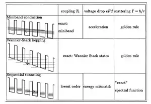
In the case of minibands, this sinusoidal character is no longer preserved. Only high up in the miniband (for wavevectors well beyond ) is the top actually 'sensed' and does the effective mass change sign. The shape of the miniband dispersion influences miniband transport profoundly and accurate dispersion relation calculations are required given wide minibands. The condition for observing single miniband transport is the absence of interminiband transfer by any process. The thermal quantum kBT should be much smaller than the energy difference between the first and second miniband, even in the presence of the applied electric field.
Bloch states
For an ideal superlattice a complete set of eigenstates states can be constructed by products of plane waves and a z-dependent function which satisfies the eigenvalue equation
- .
As and are periodic functions with the superlattice period d, the eigenstates are Bloch state with energy . Within first-order perturbation theory in k2, one obtains the energy
- .
Now, will exhibit a larger probability in the well, so that it seems reasonable to replace the second term by
where is the effective mass of the quantum well.
Wannier functions
By definition the Bloch functions are delocalized over the whole superlattice. This may provide difficulties if electric fields are applied or effects due to the superlattice's finite length are considered. Therefore, it is often helpful to use different sets of basis states that are better localized. A tempting choice would be the use of eigenstates of single quantum wells. Nevertheless, such a choice has a severe shortcoming: the corresponding states are solutions of two different Hamiltonians, each neglecting the presence of the other well. Thus these states are not orthogonal, creating complications. Typically, the coupling is estimated by the transfer Hamiltonian within this approach. For these reasons, it is more convenient to use the set of Wannier functions.
Wannier–Stark ladder
Applying an electric field F to the superlattice structure causes the Hamiltonian to exhibit an additional scalar potential eφ(z) = −eFz that destroys the translational invariance. In this case, given an eigenstate with wavefunction and energy , then the set of states corresponding to wavefunctions are eigenstates of the Hamiltonian with energies Ej = E0 − jeFd. These states are equally spaced both in energy and real space and form the so-called Wannier–Stark ladder. The potential is not bounded for the infinite crystal, which implies a continuous energy spectrum. Nevertheless, the characteristic energy spectrum of these Wannier–Stark ladders could be resolved experimentally.
Transport

The motion of charge carriers in a superlattice is different from that in the individual layers: mobility of charge carriers can be enhanced, which is beneficial for high-frequency devices, and specific optical properties are used in semiconductor lasers.
If an external bias is applied to a conductor, such as a metal or a semiconductor, typically an electric current is generated. The magnitude of this current is determined by the band structure of the material, scattering processes, the applied field strength and the equilibrium carrier distribution of the conductor.
A particular case of superlattices called superstripes are made of superconducting units separated by spacers. In each miniband the superconducting order parameter, called the superconducting gap, takes different values, producing a multi-gap, or two-gap or multiband superconductivity.
Recently, Felix and Pereira investigated the thermal transport by phonons in periodic[13] and quasiperiodic[14][15][16] superlattices of graphene-hBN according to the Fibonacci sequence. They reported that the contribution of coherent thermal transport (phonons like-wave) was suppressed as quasiperiodicity increased.
Other dimensionalities
Soon after two-dimensional electron gases (2DEG) had become commonly available for experiments, research groups attempted to create structures[17] that could be called 2D artificial crystals. The idea is to subject the electrons confined to an interface between two semiconductors (i.e. along z-direction) to an additional modulation potential V(x,y). Contrary to the classical superlattices (1D/3D, that is 1D modulation of electrons in 3D bulk) described above, this is typically achieved by treating the heterostructure surface: depositing a suitably patterned metallic gate or etching. If the amplitude of V(x,y) is large (take as an example) compared to the Fermi level, , the electrons in the superlattice should behave similarly to electrons in an atomic crystal with square lattice (in the example, these "atoms" would be located at positions (na,ma) where n,m are integers).
The difference is in the length and energy scales. Lattice constants of atomic crystals are of the order of 1Å while those of superlattices (a) are several hundreds or thousands larger as dictated by technological limits (e.g. electron-beam lithography used for the patterning of the heterostructure surface). Energies are correspondingly smaller in superlattices. Using the simple quantum-mechanically confined-particle model suggests . This relation is only a rough guide and actual calculations with currently topical graphene (a natural atomic crystal) and artificial graphene[18] (superlattice) show that characteristic band widths are of the order of 1 eV and 10 meV, respectively. In the regime of weak modulation (), phenomena like commensurability oscillations or fractal energy spectra (Hofstadter butterfly) occur.
Artificial two-dimensional crystals can be viewed as a 2D/2D case (2D modulation of a 2D system) and other combinations are experimentally available: an array of quantum wires (1D/2D) or 3D/3D photonic crystals.
Applications
The superlattice of palladium-copper system is used in high performance alloys to enable a higher electrical conductivity, which is favored by the ordered structure. Further alloying elements like silver, rhenium, rhodium and ruthenium are added for better mechanical strength and high temperature stability. This alloy is used for probe needles in probe cards.[19]
References
- Johansson; Linde (1925). "The X-ray determination of the atomic arrangement in the mixed-crystal series gold-copper and palladium-copper". Annalen der Physik. 78 (21): 439. Bibcode:1925AnP...383..439J. doi:10.1002/andp.19253832104.
- Bradley; Jay (1932). "The formation of Superlattices in Alloys if Iron and Aluminium". Proc. R. Soc. A. 136 (829): 210–232. Bibcode:1932RSPSA.136..210B. doi:10.1098/rspa.1932.0075.
- Gorsky (1928). "X-ray investigations of transformations in the CuAu alloy". Z. Phys. 50 (1–2): 64–81. Bibcode:1928ZPhy...50...64G. doi:10.1007/BF01328593. S2CID 121876817.
- Borelius (1934). "The theory of transformations of metallic mixed phases". Annalen der Physik. 20 (1): 57. Bibcode:1934AnP...412...57B. doi:10.1002/andp.19344120105.
- Dehlinger; Graf (1934). "Transformation of solid metal phases I. The tetragonal gold-copper alloy CuAu". Z. Phys. Chem. 26: 343. doi:10.1515/zpch-1934-2631. S2CID 99550940.
- Bragg, W.L.; Williams, E.J. (1934). "The effect of thermal agitation on atomic arrangement in alloys I". Proc. R. Soc. A. 145 (855): 699–730. Bibcode:1934RSPSA.145..699B. doi:10.1098/rspa.1934.0132.
- Bethe (1935). "Statistical theory of superlattices". Proc. R. Soc. A. 150 (871): 552–575. Bibcode:1935RSPSA.150..552B. doi:10.1098/rspa.1935.0122.
- Koehler, J. (1970). "Attempt to Design a Strong Solid". Physical Review B. 2 (2): 547–551. Bibcode:1970PhRvB...2..547K. doi:10.1103/PhysRevB.2.547.
- Lehoczky, S. L. (1973). "Retardation of dislocation generation and motion in thin-layered metal laminates". Acta Metallurgica. 41 (26): 1814.
- Yashar, P.; Barnett, S. A.; Rechner, J.; Sproul, W. D. (1998). "Structure and mechanical properties of polycrystalline CrN/TiN superlattices". Journal of Vacuum Science & Technology A: Vacuum, Surfaces, and Films. American Vacuum Society. 16 (5): 2913–2918. Bibcode:1998JVSTA..16.2913Y. doi:10.1116/1.581439. ISSN 0734-2101.
- Esaki, L.; Tsu, R. (1970). "Superlattice and Negative Differential Conductivity in Semiconductors". IBM Journal of Research and Development. 14: 61–65. doi:10.1147/rd.141.0061.
- Gorbachev, R. V.; Song, J. C. W.; Yu, G. L.; Kretinin, A. V.; Withers, F.; Cao, Y.; Mishchenko, A.; Grigorieva, I. V.; Novoselov, K. S.; Levitov, L. S.; Geim, A. K. (2014). "Detecting topological currents in graphene superlattices". Science. 346 (6208): 448–451. arXiv:1409.0113. Bibcode:2014Sci...346..448G. doi:10.1126/science.1254966. PMID 25342798. S2CID 2795431.
- Felix, Isaac M.; Pereira, Luiz Felipe C. (9 February 2018). "Thermal Conductivity of Graphene-hBN Superlattice Ribbons". Scientific Reports. 8 (1): 2737. Bibcode:2018NatSR...8.2737F. doi:10.1038/s41598-018-20997-8. PMC 5807325. PMID 29426893.
- Felix, Isaac M.; Pereira, Luiz Felipe C. (30 April 2020). "Suppression of coherent thermal transport in quasiperiodic graphene-hBN superlattice ribbons". Carbon. 160: 335–341. arXiv:2001.03072. doi:10.1016/j.carbon.2019.12.090. S2CID 210116531.
- Felix, Isaac M.; Pereira, Luiz Felipe C. (1 May 2022). "Thermal conductivity of Thue–Morse and double-period quasiperiodic graphene-hBN superlattices". International Journal of Heat and Mass Transfer. Elsevier. 186: 122464. doi:10.1016/j.ijheatmasstransfer.2021.122464. S2CID 245712349.
- Félix, Isaac de Macêdo (4 August 2020). "Condução de calor em nanofitas quase-periódicas de grafeno-hBN" (in Brazilian Portuguese).
- Heitmann, D.; Kotthaus, J. R. P. (1993). "The Spectroscopy of Quantum Dot Arrays". Physics Today. 46 (6): 56. Bibcode:1993PhT....46f..56H. doi:10.1063/1.881355.
- Kato, Y.; Endo, A.; Katsumoto, S.; Iye, Y. (2012). "Geometric resonances in the magnetoresistance of hexagonal lateral superlattices". Physical Review B. 86 (23): 235315. arXiv:1208.4480. Bibcode:2012PhRvB..86w5315K. doi:10.1103/PhysRevB.86.235315. S2CID 119289481.
- "United States Patent US10385424B2 Palladium-based alloys" (PDF). google patents. Retrieved 19 June 2020.
- H.T. Grahn, "Semiconductor Superlattices", World Scientific (1995). ISBN 978-981-02-2061-7
- Schuller, I. (1980). "New Class of Layered Materials". Physical Review Letters. 44 (24): 1597–1600. Bibcode:1980PhRvL..44.1597S. doi:10.1103/PhysRevLett.44.1597.
- Morten Jagd Christensen, "Epitaxy, Thin Films and Superlattices", Risø National Laboratory, (1997). ISBN 8755022987 Superlattice at Google Books
- C. Hamaguchi, "Basic Semiconductor Physics", Springer (2001). Superlattice at Google Books ISBN 3540416390
- Wacker, A. (2002). "Semiconductor superlattices: A model system for nonlinear transport". Physics Reports. 357 (1): 1–7. arXiv:cond-mat/0107207. Bibcode:2002PhR...357....1W. CiteSeerX 10.1.1.305.3634. doi:10.1016/S0370-1573(01)00029-1. S2CID 118885849.
- Haugan, H. J.; Szmulowicz, F.; Mahalingam, K.; Brown, G. J.; Munshi, S. R.; Ullrich, B. (2005). "Short-period InAs/GaSb type-II superlattices for mid-infrared detectors". Applied Physics Letters. 87 (26): 261106. Bibcode:2005ApPhL..87z1106H. doi:10.1063/1.2150269.
Further reading
- Mendez, E. E.; Bastard, G. R. (1993). "Wannier-Stark Ladders and Bloch Oscillations in Superlattices". Physics Today. 46 (6): 34–42. Bibcode:1993PhT....46f..34M. doi:10.1063/1.881353.