Tape-automated bonding
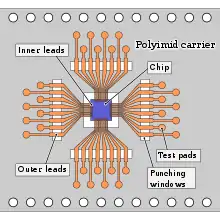
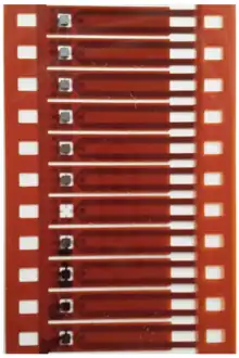
Tape-automated bonding (TAB) is a process that places bare semiconductor chips (dies) like integrated circuits onto a flexible circuit board (FPC) by attaching them to fine conductors in a polyamide or polyimide (like trade names Kapton or UPILEX) film carrier. This FPC with the die(s) (TAB inner lead bonding, ILB) can be mounted on the system or module board or assembled inside a package (TAB outer lead bonding, OLB). Typically the FPC includes from one to three conductive layers and all inputs and outputs of the semiconductor die are connected simultaneously during the TAB bonding. [1][2][3] Tape automated bonding is one of the methods needed for achieving chip-on-flex (COF) assembly and it is one of the first roll-to-roll processing (also called R2R, reel-to-reel) type methods in the electronics manufacturing.

Process
The TAB mounting is done such that the bonding sites of the die, usually in the form of bumps or balls made of gold, solder or anisotropic conductive material, are connected to fine conductors on the tape, which provide the means of connecting the die to the package or directly to external circuits. The bumps or balls can locate either on the die or on the TAB tape. TAB compliant metallizations systems are:[4]
- Al pads on the die < - > gold plated Cu on tape areas (thermosonic bonding)
- Al covered with Au on pads on the die < - > Au or Sn bumped tape areas (gang bonding)
- Al pads with Au bumps on the die < - > Au or Sn plated tape areas (gang bonding)
- Al pads with solder bumps on the die < - > Au, Sn or solder plated tape areas (gang bonding)
Sometimes the tape on which the die is bonded already contains the actual application circuit of the die.[5] The film is moved to the target location, and the leads are cut and joining the chip takes place as necessary. There are several joining methods used with TAB: thermocompression bonding (with help of a pressure, sometimes called as a gang bonding), thermosonic bonding etc. The bare chip may then be encapsulated ("glob topped") with epoxy or similar.[6]

The merits of the tape-automated bonding are:
- All chip interconnections (inputs/outputs from/to the chip) are made during one bonding, and this differentiates TAB from the wire bonding.
- This bonding technique can be highly automated, and if needed very fast. Therefore TAB is used in high volume electronics production.
- Produces very light and thin assembly, because of the thin substrate and minimum possible glob topping covering only the chip area. There are many applications like in sensory, in medical, space electronics, bank and credit cards, SIM cards of portable equipment like mobile phones etc. where thin assembly with small weight are beneficial.
- In some applications additional packaging possibly may not be needed and it may replace the metallic lead frame in some packaging approaches.
The challenges of the tape-automated bonding are:
- Specific machinery is needed in the manufacturing.[7]
- Chips need to have bumps on the input/output (IO) pads or bumps need to be on the tape. The bumps and metals on the chip and on the tape must be compliant for achieving reliable in all environmental and other circumstances of the application.[8]
- Interconnection methods - TAB and flip chip - are enabling all IOs of the chip to be interconnected at the same time. Therefore the speed advantage of TAB has diminished with the development of the flip chip manufacturing, because flip chip uses soldering which also with the time has developed towards fine pitch interconnection method similar to TAB. Additionally speed up of the wire bonding has left TAB to be mostly applied in some specific areas like display driver interconnections and smart cards. Although TAB is a viable high speed and high density[9] interconnection method.
Standards
Standard sizes for polyimide tapes include widths of 35 mm, 45 mm, and 70 mm and thicknesses between 50 and 100 micrometers. Since the tape is in the form of a roll, the length of the circuit is measured in terms of sprocket pitches, with each sprocket pitch measuring about 4.75 mm. Thus, a circuit size of 16 pitches is about 76 mm long.
History and background
Technically the process was invented by Frances Hugle -patent issued 1969 - although it was not named as TAB.[10] The TAB was first outlined by Gerard Dehaine 1971 at Honeywell Bull.[11] Historically, TAB was created as an alternative to wire bonding and finds common use by electronics manufacturers.[12] However speed up of wire bonding methods and development of flip chip - enabling simultaneous bonding of all IOs of the die and easier repaire compared to TAB - have pushed TAB bonding to be used in specific areas like for interconnection of display drivers to the display like liquid crystal display (LCD).
References
- "Lecture: Interconnection in IC assembly" (PDF).
- Greig, W. J. (2007). Integrated Circuit Packaging, Assembly and Interconnections. Springer. pp. 129–142. ISBN 978-0-387-28153-7.
- Lau, J. H. (1982). Handbook of Tape Automated Bonding 645 p. Springer. ISBN 978-0442004279.
- "Roadmaps of Packaging Technology, Integrated circuit Engineering, Chapter 9 (editors D. Potter and L. Peters), Chip bonding at the first level, 9-1...9-38" (PDF).
- "TAB at Silicon Far East on-line".
- "Tape-Automated Bonding". Centre for High Performance Integrated Technologies and Systems (CHIPTEC). March 1997.
- Lai, J.K.L.; et., al. (1995). "Effects of bond temperature and pressure on microstructures of tape automated bonding (TAB) inner lead bonds (ILB) with thin tape metallization". 1995 Proceedings. 45th Electronic Components and Technology Conference. pp. 819–826. doi:10.1109/ECTC.1995.517782. ISBN 0-7803-2736-5. S2CID 136639010.
- Yan-Xiang, K.; Ling, L. (1990). "Tape bump forming and bonding in BTAB". 40th Conference Proceedings on Electronic Components and Technology. 2: 943–947. doi:10.1109/ECTC.1990.122302. S2CID 110303672.
- Kurzweil, K.; Dehaine, G. (1982). "Density Upgrade in Tape Automated Bonding". Electrocomponent Science and Technology, Gordon and Breach Science Publishers, Inc. 10: 51–55.
- "Patent US3440027 Automated packaging of Semiconductors".
- "Tape Automated Bonding" (PDF).
- "Tape Automated Bonding (TAB)". Advantest Europe Customer Newsletter. Advantest GmbH.