Transfer length method
The Transfer Length Method or the "Transmission Line Model" (both abbreviated as TLM) is a technique used in semiconductor physics and engineering to determine the specific contact resistivity between a metal and a semiconductor.[1][2][3] TLM has been developed because with the ongoing device shrinkage in microelectronics the relative contribution of the contact resistance at metal-semiconductor interfaces in a device could not be neglected any more and an accurate measurement method for determining the specific contact resistivity was required.[4]
General description
The goal of the transfer length method (TLM) is the determination of the specific contact resistivity of a metal-semiconductor junction. To create a metal-semiconductor junction a metal film is deposited on the surface of a semiconductor substrate. The TLM is usually used to determine the specific contact resistivity when the metal-semiconductor junction shows ohmic behaviour. In this case the contact resistivity can be defined as the voltage difference across the interfacial layer between the deposited metal and the semiconductor substrate divided by the current density which is defined as the current divided by the interfacial area through which the current is passing:[5]
In this definition of the specific contact resistivity refers to the voltage value just below the metal-semiconductor interfacial layer while represents the voltage value just above the metal-semiconductor interfacial layer. There are two different methods of performing TLM measurements which are both introduced in the remainder of this section. One is called just transfer length method while the other is named circular transfer length method (c-TLM).[1]
TLM
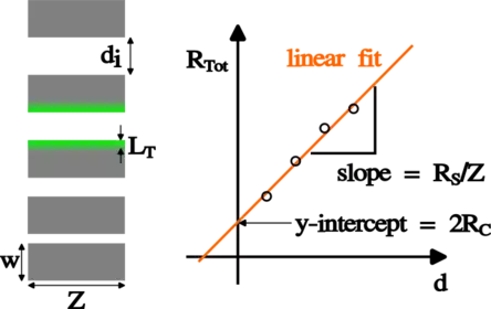
To determine the specific contact resistivity an array of rectangular metal pads is deposited on the surface of a semiconductor substrate as it is depicted in the image to the right. The definition of the rectangular pads can be done by utilizing photolithography while the metal deposition can be done with sputter deposition, thermal evaporation or electroless deposition.[6][7]
In the image to the right the distance between the pads increases from the bottom to the top. Therefore, when the resistance between adjacent pads is measured the total resistance increases accordingly as it is indicated in the graph beneath the depiction of the metal pads. In this graph the abscissa represents the distance between two adjacent metal pads while the circles represent measured resistance values. The total resistivity can be separated into a component due to the uncovered semiconductor substrate and a component that corresponds to the voltage drop in two metal-covered areas. The former component can be described with the formula , whereas represents the sheet resistance of the semiconductor substrate and the width of the metal pads. The other component that contributes to the total resistance is denoted by because when two adjacent pads are characterized two identical metallized areas have to be considered. This means that the total resistance can be written in the following functional form, with the pad distance as independent variable:
If the contribution of the metal layer itself is neglected then arises because of the voltage drop at the metal-semiconductor interface as well as in the semiconductor substrate underneath. This means that during a total resistance measurement, the voltage drops exponentially (and hence also the current density) in the metallic regions (see also theory section for further explanation).[8] As it is derived in the next section of this article the majority of the voltage drop underneath a metallic pad takes place within in the length which is defined as the transfer length .[1][4][8] Metaphorically speaking this means that the main part of the area underneath a metallic contact through which current enters the metal via the metal-semiconductor interface is given by the transfer length multiplied with the width of the pad . This situation is also depicted in the figure in this section where the current density distribution underneath two adjacent metal pads during a resistance measurement is depicted with a green colouring. All in all this means that (if the metal pad length is much larger than the transfer length) that a relation between and can be stated:[3][4]
Since can be extracted from a linear fit through the data points and can be obtained from the y-intercept of the linear fit an estimation of is possible.
Circular TLM
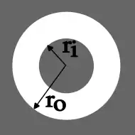
The original TLM method as described above has the drawback, that the current does not just flow within the area given by times . This means that the current density distribution also spreads to the vertical sides of the metallic pads in the figure in the TLM section, a phenomenon that is not considered in the derivation of the formula describing .[4][1] To account for this geometrical issue instead of rectangular metallic pads, circular pads with radius are used which are separated from a holohedral metallic coating by a distance (see figure to the right). When the total resistance between circular pad and holohedral coating is measured three distinguishable components contribute to the measured value, namely the gap resistance and the contact resistances at the inner and outer end of the gap area ( and ). This is expressed in the following formula:
As will be derived in the theory section an expression for that allows the extraction of from experimental data as long as is much larger than :
Similar to the TLM method and can be obtained with a multiple linear regression analysis utilizing data-pairs of and .[1]
Theory
TLM
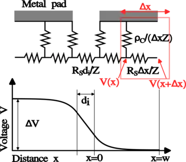
In the last section the basic principle of TLM was introduced and now more details about the theoretical background are given. The main purpose here is to find an expression that relates the measurable quantity with the specific contact resistivity which is intended to be determined with TLM. Therefore, in the image to the right a resistor network is illustrated that describes the situation when a voltage is applied between two adjacent metallic pads. The resistor () in the middle takes account for the part that is not covered with metal while the rest describes the situation for the metallic pads. The horizontal resistor elements () represent the resistance due to the semiconductor substrate and the vertical resistor elements () take account for the resistance due to the metal-semiconductor interfacial layer. In this description pairs of horizontal and vertical resistor elements describe the situation within a volume element of length in a metallic pad area. This methodology is also used for the derivation of the telegrapher's equations which are used to describe the behaviour of transmission lines. Because of this analogy, the described measurement technique in this article is often called the transmission line method.[1]
By using Kirchhoff's circuit laws the following expressions for the voltage as well as for the current within the above considered length element (read square in the figure in this section) are obtained for a steady state situation where both voltage and current are not a function of time:
By taking the limit the following two differential equations are obtained:[9]
These two coupled differential equations can be separated by differentiating one with respect to such that the other can plugged in. By doing so finally, two differential equations are obtained which do not depend on each other:
Both differential equations have solutions of the form whereat and are constants which need to be determined by using appropriate boundary conditions and is given by . Two boundary conditions can be obtained by defining the voltage as well as the current at the beginning of a metallic pad area as and respectively. In a formal manner this means that and when using the settings in the figure in this section. By using the pair of coupled differential equations above two more boundary conditions are obtained, namely and which is the inverse of the previously defined transfer length . Eventually two equations, describing the voltage and the current as a function of distance are obtained by using the four stated boundary conditions:[4]
When a measurement is performed, it can be assumed that no current is flowing at the opposing end of each metallic pad, which in turn means that . This allows a further refinement of the equation describing the voltage when using the relation :
The last equation describes the voltage drop across the region covered by a metallic pad (compare with the figure in this section). By realizing that the resistance value can be expressed with and by setting in the last formula an expression can be found that relates to the specific contact resistivity :
The last equation allows the calculation of by utilizing experimental data. Since goes to 1 as increases and is significantly larger than the transfer length often the estimation is used instead of the strictly derived equality. This is identical to what was stated in the general description section.[3][8][4] In summary the voltage as well as the current as a function of distance in the region of a metallic pad has been derived by utilizing a model that is similar to the telegrapher's equations. This enabled to find an expression that allows the calculation of the specific contact resistivity of the metal-semiconductor junction by using the experimentally found quantities and and the width of a metallic pad.
Circular TLM
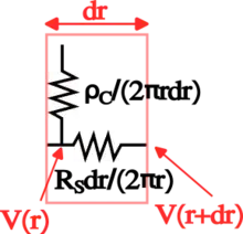
The physical idea of deriving differential equations for the c-TLM method is the same as for TLM but polar coordinates are used instead of cartesian coordinates. This changes the resistor network that describes the metal covered area as can be seen in the figure to the right. Like for TLM by using Kirchhoff's circuit laws two coupled differential equations are obtained.
When the current is eliminated a different equation for the voltage is obtained:[10]
A general solution to this type of differential equations is given as follows, whereat and are unspecified constants and is . The functions and are zero-order modified Bessel functions of the first and second kind respectively.[11]
By utilizing the coupled differential equations above and the differentiation rules for modified Bessel functions (, )[11] an expression for the current can be obtained. The functions and are first-order Bessel functions of the first and second kind respectively.
.svg.png.webp)
.svg.png.webp)
Now after having obtained expressions for the current as well as for the voltage, expressions for the contact resistances corresponding to the inner and outer boundary of the gap area have to be found (compare with the schematic illustration of the measurement metallization in the general section). The contact resistance at the inner boundary is given by and during a measurement the current in the middle of the circular metallic pad is zero (). Since the modified Bessel function tends to infinity when tends to zero (see figures to the right), the constant has to be zero because the voltage can not be infinite. Considering this, the contact resistance at the inner boundary of the gap area equates to:
In a similar manner an expression for the contact resistance at the outer boundary of the gap area can be found when is replaced with (compare with the drawing in the general section). Here, also a boundary condition for the current can be given, namely . This means that A has to be zero because the function tends to infinity (see figure to the right) as goes to infinity. In turn this means that the contact resistance at the outer boundary of the gap area is given by:
The resistance due to the gap area itself can be found by considering the horizontal differential resistor in the figure in this section and by integrating from to . By adding , and an expression for the total resistance can be given:
When the outer and the inner radius are much larger than the transfer length the quotients of the modified Bessel functions are approximately one.[1] This means that when is substituted with the same formula for as given in the general section is found, which can be used for extracting and from experimental data:
Practical example
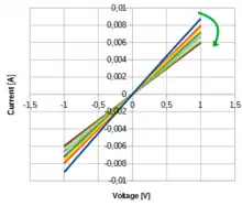
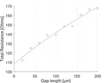
In this section a practical example of a c-TLM measurement is presented. By utilizing photolithography and sputter deposition, metallic c-TLM pads were deposited on the surface of a semiconductor thin film. The gap spacings of the c-TLM pads ranged between 20 µm and 200 µm while step sizes of 20 µm where chosen. To obtain values for the total resistance corresponding to each c-TLM pad, current-voltage measurements were performed across each gap spacing. The plot to the left shows the recorded measurement data, whereat the green arrow indicates an increase of the gap length. The curves are linear (which proofs that there is an ohmic contact between the metal and semiconductor layer) and the value of the total resistance for each c-TLM pad is obtained by taking the inverse of the slope.
For the extraction of , and the specific contact resistivity the equation obtained for the total resistance is re-written as follows, with , , and :
- .
This re-writing was done to compactify the notation and also because in this particular example the inner diameter was kept constant for each c-TLM pad. Since 10 measurements of were performed -each corresponding to a different gap length - a system of linear equations can be obtained, which can be written in matrix-vector form.
The vector on the left side contains the values from the resistance measurements , all of them exhibiting a measurement error . Therefore a measurement error vector is added to the matrix-vector product. Before proceeding the matrix-vector equation is written in a more compact form:
The goal is to find values of and such that the euclidean norm of the error vector becomes minimal. With this premise the error vector must be normal to the column space of , which means that .[12] This means, that multiplication of the matrix-vector equation with the transposed matrix of yields:
- .
Since all components of can be calculated and the components of are provided by the resistance measurements, the coefficients and can be calculated. Finally from the two coefficients, the values for , and the specific contact resistivity can be calculated as well. A plot to the left shows the measured resistance values in dependence of the gap length together with the fitting function corresponding to the determined coefficients and .
The following GNU Octave script corresponds to the performed measurement series and also includes the obtained resistance values. A plot of the measurement points together with the fitting function is created and the values for , and the specific contact resistivity are calculated as well.
%vectors that contain the obtained measurement data
d = 20:20:200; #this vector contains the gap lengths
R_row = [112.258772, 125.071437, 130.619235, 138.959548, 139.110758, 148.420932, 148.474871, 160.83128, 166.670412, 167.614947];
R = transpose(R_row);

%Here the column vectors of X are defined
r_i = 200;
x1 = transpose(log((r_i.+d)/r_i));
x2 = transpose(1./(r_i.+d) + 1/r_i);

%Define the matrix X
X = [x1, x2];

%Obtain the values A and B
beta = inv(transpose(X)*X)*transpose(X)*R;
A = beta(1);
B = beta(2);

%Define the fitting function
d_fit = 0:1:200;
R_fit = A*log((r_i.+d_fit)/r_i) + B*(1./(r_i.+d_fit) + 1/r_i);

%Plot the fitting function and the measurement values
scatter(d,R, "r");
hold on;
plot(d_fit, R_fit);
set(gca,'fontsize',14);
xlabel('Gap length [µm]');
ylabel('Total Resistance [Ohms]');

%Calculate the physical properties
R_S = A*2*pi; #given in ohms
L_T = 2*pi*B/R_S; #given in µm
rho_c = (R_S*(L_T)^2)*10^(-8); #given in Ohm*cm^2
See also
- Four-terminal sensing – Method of measuring electrical impedance
- Van der Pauw method – An accurate way to measure resistance and hall voltage
References
- Cohen, SS; Gildenblatt, G Sh. (1986). Chapter 4 - Test Structures for Ohmic Contact Characterization. VLSI Electronics Microstructure Science Volume 13 Chapter 4. Elsevier. ISBN 9780122341137.
- Williams, Ralph (1990). Modern GaAs Processing Methods. Artech House. ISBN 0890063435.
- Schroder, Dieter K. (2006). Semiconductor Material and Device Characterization. John Wiley & Sons. ISBN 0471739065.
- Berger HH (June 1971). "Models for contacts to planar devices". Solid State Electronics. 15 (2): 145–158. doi:10.1016/0038-1101(72)90048-2.
- Saraswat K. "Lecture notes EE311 Advanced Integrated Circuit Fabrication Processes Stanford University" (PDF). web.stanford.edu.
- Porter L, Davis RF (May 1995). "A critical review of ohmic and rectifying contacts for silicon carbide" (PDF). Materials Science and Engineering: B. 34 (2–3): 83–105. doi:10.1016/0921-5107(95)01276-1.
- Braun S, Emre E, Raabe B, Hahn G (September 2010). Electroless nickel and copper metallization : Contact formation on crystalline silicon and background plating behavior on PECVD silicon SiNx:H layers (PDF). 25th European Photovoltaic Solar Energy Conference and Exhibition. 5th World Conference on photovoltaic Energy Conversion. Valencia, Spain. pp. 1892–1895. doi:10.4229/25thEUPVSEC2010-2CV.2.51.
- Marlow GS, Murkund BD (1982). "The Effects of Contact Size and non-zero Metal Resistance on the Determination of specific contact resistance". Solid State Electronics. 25 (2): 91–84. Bibcode:1982SSEle..25...91M. doi:10.1016/0038-1101(82)90036-3.
- Peterson AF, Durgin GD (2009). Transient Signals on Transmission Lines. Morgan & Claypool Publishers. ISBN 9781598298253.
- Reeves GK (1979). "Specific Contact Resistance using a circular Transmission Line Model". Solid State Electronics. 23 (5): 487–490. doi:10.1016/0038-1101(80)90086-6.
- McLachlan, N.W. (1954). Bessel Functions for Engineers. Oxford University Press. ISBN 1124148620.
- Strang, Gilbert (2016). Introduction to linear algebra (Fifth ed.). Wellesley, MA: Wellesley-Cambridge Press. pp. 128, 168. ISBN 978-0-9802327-7-6. OCLC 956503593.
Further reading
- Gary Tuttle, Dept. of Electrical and Computer Engineering, Iowa State University. "Contact resistance and TLM measurements" (PDF).
{{cite web}}: CS1 maint: multiple names: authors list (link)