Two-dimensional semiconductor
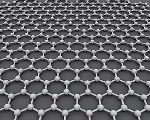
A two-dimensional semiconductor (also known as 2D semiconductor) is a type of natural semiconductor with thicknesses on the atomic scale. Geim and Novoselov et al. initiated the field in 2004 when they reported a new semiconducting material graphene, a flat monolayer of carbon atoms arranged in a 2D honeycomb lattice.[1] A 2D monolayer semiconductor is significant because it exhibits stronger piezoelectric coupling than traditionally employed bulk forms. This coupling could enable applications.[2] One research focus is on designing nanoelectronic components by the use of graphene as electrical conductor, hexagonal boron nitride as electrical insulator, and a transition metal dichalcogenide as semiconductor.[3][4]
Materials
Graphene
Graphene, consisting of single sheets of carbon atoms, has high electron mobility and high thermal conductivity. One issue regarding graphene is its lack of a band gap, which poses a problem in particular with digital electronics because it is unable to switch off field-effect transistors (FETs).[3]
-side-3D-balls.png.webp)
Hexagonal boron nitride
Monolayer hexagonal boron nitride (h-BN) is an insulator with a high energy gap (5.97 eV).[5] However, it can also function as a semiconductor with enhanced conductivity due to its zigzag sharp edges and vacancies. h-BN is often used as substrate and barrier due to its insulating property. h-BN also has a large thermal conductivity.
Transition-metal dichalcogenides
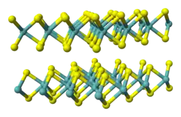
Transition-metal dichalcogenide monolayers (TMDs or TMDCs) are a class of two-dimensional materials that have the chemical formula MX2, where M represents transition metals from group VI, V and VI, and X represents a chalcogen such as sulfur, selenium or tellurium.[6] MoS2, MoSe2, MoTe2, WS2 and WSe2 are TMDCs. TMDCs have layered structure with a plane of metal atoms in between two planes of chalcogen atoms as shown in Figure 1. Each layer is bonded strongly in plane, but weakly in interlayers. Therefore, TMDCs can be easily exfoliated into atomically thin layers through various methods. TMDCs show layer-dependent optical and electrical properties. When exfoliated into monolayers, the band gaps of several TMDCs change from indirect to direct,[7] which lead to broad applications in nanoelectronics,[3] optoelectronics,[8][9] and quantum computing.[10]
III-IV chalcogenides
Another class of 2D semiconductors are III-IV chalcogenides. These materials have the chemical formula MX, where M is a metal from group 13 (Ga, In) and X is a chalcogen atom (S, Se, Te). Typical members of this group are InSe and GaSe, both of which have shown high electronic mobilities and band gaps suitable for a wide range of electronic applications.[11][12]
Synthesis
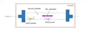
2D semiconductor materials are often synthesized using a chemical vapor deposition (CVD) method. Because CVD can provide large-area, high-quality, and well-controlled layered growth of 2D semiconductor materials, it also allows synthesis of two-dimensional heterojunctions.[13] When building devices by stacking different 2D materials, mechanical exfoliation followed by transferring is often used.[4][6] Other possible synthesis methods include electrochemical deposition,[14][15] chemical exfoliation, hydrothermal synthesis, and thermal decomposition. In 2008 cadmium selenide CdSe quasi 2D platelets were first synthesized by colloidal method with thicknesses of several atomic layers and lateral sizes up to dozens of nanometers.[16] Modification of the procedure allowed to obtain other nanoparticles with different compositions (like CdTe,[17] HgSe,[18] CdSexS1−x alloys,[19] core/shell[20] and core/crown [21] heterostructures) and shapes (as scrolls,[22] nanoribbons,[23] etc).
Proposed applications
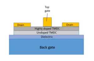
Some applications include electronic devices,[25] photonic and energy harvesting devices, and flexible and transparent substrates.[3] Other applications include on quantum computing qubit devices[10] solar cells,[26] and flexible electronics.[6]
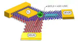
Quantum computing
Theoretical work has predicted the control of the band edges hybridization on some van der Waals heterostructures via electric fields and proposed its usage in quantum bit devices, considering the ZrSe2/SnSe2 heterobilayer as an example.[10] Further experimental work has confirmed these predictions for the case of the MoS2/WS2 heterobilayer.[27]
Magnetic NEMS
2D layered magnetic materials are attractive building blocks for nanoelectromechanical systems (NEMS): while they share high stiffness and strength and low mass with other 2D materials, they are magnetically active. Among the large class of newly emerged 2D layered magnetic materials, of particular interest is few-layer CrI3, whose magnetic ground state consists of antiferromagnetically coupled ferromagnetic (FM) monolayers with out-of-plane easy axis. The interlayer exchange interaction is relatively weak, a magnetic field on the order of 0.5 T in the out-of-plane (𝒛) direction can induce spin-flip transition in bilayer CrI3. Remarkable phenomena and device concepts based on detecting and controlling the interlayer magnetic state have been recently demonstrated, including spin-filter giant magnetoresistance, magnetic switching by electric field or electrostatic doping, and spin transistors. The coupling between the magnetic and mechanical properties in atomically thin materials, the basis for 2D magnetic NEMS, however, remains elusive although NEMS made of thicker magnetic materials or coated with FM metals have been studied.
References
- Novoselov, K. S. (2004). "Electric Field Effect in Atomically Thin Carbon Films". Science. 306 (5696): 666–669. arXiv:cond-mat/0410550. Bibcode:2004Sci...306..666N. doi:10.1126/science.1102896. ISSN 0036-8075. PMID 15499015. S2CID 5729649.
- Song, Xiufeng; Hu, Jinlian; Zeng, Haibo (2013). "Two-dimensional semiconductors: recent progress and future perspectives". Journal of Materials Chemistry C. 1 (17): 2952. doi:10.1039/C3TC00710C.
- Radisavljevic, B.; Radenovic, A.; Brivio, J.; Giacometti, V.; Kis, A. (2011). "Single-layer MoS2 transistors". Nature Nanotechnology. 6 (3): 147–150. Bibcode:2011NatNa...6..147R. doi:10.1038/nnano.2010.279. PMID 21278752.
- Geim, A. K.; Grigorieva, I. V. (2013). "Van der Waals heterostructures". Nature. 499 (7459): 419–425. arXiv:1307.6718. doi:10.1038/nature12385. ISSN 0028-0836. PMID 23887427. S2CID 205234832.
- Dean, C. R.; Young, A. F.; Meric, I.; Lee, C.; Wang, L.; Sorgenfrei, S.; Watanabe, K.; Taniguchi, T.; Kim, P.; Shepard, K. L.; Hone, J. (2010). "Boron nitride substrates for high-quality graphene electronics". Nature Nanotechnology. 5 (10): 722–726. arXiv:1005.4917. Bibcode:2010NatNa...5..722D. doi:10.1038/nnano.2010.172. ISSN 1748-3387. PMID 20729834. S2CID 1493242.
- Wang, Qing Hua; Kalantar-Zadeh, Kourosh; Kis, Andras; Coleman, Jonathan N.; Strano, Michael S. (2012). "Electronics and optoelectronics of two-dimensional transition metal dichalcogenides". Nature Nanotechnology. 7 (11): 699–712. Bibcode:2012NatNa...7..699W. doi:10.1038/nnano.2012.193. ISSN 1748-3387. PMID 23132225. S2CID 6261931.
- Kuc, A.; Zibouche, N.; Heine, T. (2011). "Influence of quantum confinement on the electronic structure of the transition metal sulfideTS2". Physical Review B. 83 (24): 245213. arXiv:1104.3670. Bibcode:2011PhRvB..83x5213K. doi:10.1103/PhysRevB.83.245213. ISSN 1098-0121. S2CID 119112827.
- Wilson, J.A.; Yoffe, A.D. (1969). "The transition metal dichalcogenides discussion and interpretation of the observed optical, electrical and structural properties". Advances in Physics. 18 (73): 193–335. Bibcode:1969AdPhy..18..193W. doi:10.1080/00018736900101307. ISSN 0001-8732.
- Yoffe, A D (1973). "Layer Compounds". Annual Review of Materials Science. 3 (1): 147–170. Bibcode:1973AnRMS...3..147Y. doi:10.1146/annurev.ms.03.080173.001051. ISSN 0084-6600.
- B. Lucatto; et al. (2019). "Charge qubit in van der Waals heterostructures". Physical Review B. 100 (12): 121406. arXiv:1904.10785. Bibcode:2019PhRvB.100l1406L. doi:10.1103/PhysRevB.100.121406. S2CID 129945636.
- Arora, Himani; Jung, Younghun; Venanzi, Tommaso; Watanabe, Kenji; Taniguchi, Takashi; Hübner, René; Schneider, Harald; Helm, Manfred; Hone, James C.; Erbe, Artur (2019-11-20). "Effective Hexagonal Boron Nitride Passivation of Few-Layered InSe and GaSe to Enhance Their Electronic and Optical Properties". ACS Applied Materials & Interfaces. 11 (46): 43480–43487. doi:10.1021/acsami.9b13442. hdl:11573/1555190. ISSN 1944-8244. PMID 31651146. S2CID 204884014.
- Arora, Himani; Erbe, Artur (2021). "Recent progress in contact, mobility, and encapsulation engineering of InSe and GaSe". InfoMat. 3 (6): 662–693. doi:10.1002/inf2.12160. ISSN 2567-3165. S2CID 228902032.
- Duan, Xidong; Wang, Chen; Shaw, Jonathan C.; Cheng, Rui; Chen, Yu; Li, Honglai; Wu, Xueping; Tang, Ying; Zhang, Qinling; Pan, Anlian; Jiang, Jianhui; Yu, Ruqing; Huang, Yu; Duan, Xiangfeng (2014). "Lateral epitaxial growth of two-dimensional layered semiconductor heterojunctions". Nature Nanotechnology. 9 (12): 1024–1030. Bibcode:2014NatNa...9.1024D. doi:10.1038/nnano.2014.222. ISSN 1748-3387. PMID 25262331.
- Noori, Yasir J.; Thomas, Shibin; Ramadan, Sami; Smith, Danielle E.; Greenacre, Vicki K.; Abdelazim, Nema; Han, Yisong; Beanland, Richard; Hector, Andrew L.; Klein, Norbert; Reid, Gillian; Bartlett, Philip N.; Kees de Groot, C. H. (2020-11-04). "Large-Area Electrodeposition of Few-Layer MoS 2 on Graphene for 2D Material Heterostructures". ACS Applied Materials & Interfaces. 12 (44): 49786–49794. doi:10.1021/acsami.0c14777. ISSN 1944-8244. PMID 33079533. S2CID 224828493.
- Noori, Y J; Thomas, S; Ramadan, S; Greenacre, V K; Abdelazim, N M; Han, Y; Zhang, J; Beanland, R; Hector, A L; Klein, N; Reid, G; Bartlett, P N; de Groot, C H (2022-01-01). "Electrodeposited WS 2 monolayers on patterned graphene". 2D Materials. 9 (1): 015025. arXiv:2109.00083. Bibcode:2022TDM.....9a5025N. doi:10.1088/2053-1583/ac3dd6. ISSN 2053-1583. S2CID 244693600.
- Ithurria, Sandrine; Dubertret, Benoit (2008-12-10). "Quasi 2D Colloidal CdSe Platelets with Thicknesses Controlled at the Atomic Level". Journal of the American Chemical Society. 130 (49): 16504–16505. doi:10.1021/ja807724e. ISSN 0002-7863. PMID 19554725.
- Pedetti, Silvia; Nadal, Brice; Lhuillier, Emmanuel; Mahler, Benoit; Bouet, Cécile; Abécassis, Benjamin; Xu, Xiangzhen; Dubertret, Benoit (2013-06-25). "Optimized Synthesis of CdTe Nanoplatelets and Photoresponse of CdTe Nanoplatelets Films". Chemistry of Materials. 25 (12): 2455–2462. doi:10.1021/cm4006844. ISSN 0897-4756. S2CID 101411815.
- Izquierdo, Eva; Dufour, Marion; Chu, Audrey; Livache, Clément; Martinez, Bertille; Amelot, Dylan; Patriarche, Gilles; Lequeux, Nicolas; Lhuillier, Emmanuel; Ithurria, Sandrine (2018-06-26). "Coupled HgSe Colloidal Quantum Wells through a Tunable Barrier: A Strategy To Uncouple Optical and Transport Band Gap". Chemistry of Materials. 30 (12): 4065–4072. doi:10.1021/acs.chemmater.8b01028. ISSN 0897-4756. S2CID 103490948.
- Fan, Fengjia; Kanjanaboos, Pongsakorn; Saravanapavanantham, Mayuran; Beauregard, Eric; Ingram, Grayson; Yassitepe, Emre; Adachi, Michael M.; Voznyy, Oleksandr; Johnston, Andrew K.; Walters, Grant; Kim, Gi-Hwan (2015-07-08). "Colloidal CdSe1–xSx Nanoplatelets with Narrow and Continuously-Tunable Electroluminescence". Nano Letters. 15 (7): 4611–4615. Bibcode:2015NanoL..15.4611F. doi:10.1021/acs.nanolett.5b01233. ISSN 1530-6984. PMID 26031416.
- Mahler, Benoit; Nadal, Brice; Bouet, Cecile; Patriarche, Gilles; Dubertret, Benoit (2012-11-14). "Core/Shell Colloidal Semiconductor Nanoplatelets". Journal of the American Chemical Society. 134 (45): 18591–18598. doi:10.1021/ja307944d. ISSN 0002-7863. PMID 23057684.
- Kelestemur, Yusuf; Olutas, Murat; Delikanli, Savas; Guzelturk, Burak; Akgul, Mehmet Zafer; Demir, Hilmi Volkan (2015-01-29). "Type-II Colloidal Quantum Wells: CdSe/CdTe Core/Crown Heteronanoplatelets". The Journal of Physical Chemistry C. 119 (4): 2177–2185. doi:10.1021/jp510466k. hdl:11693/23136. ISSN 1932-7447.
- Vasiliev, Roman B.; Lazareva, Elizabeth P.; Karlova, Daria A.; Garshev, Alexey V.; Yao, Yuanzhao; Kuroda, Takashi; Gaskov, Alexander M.; Sakoda, Kazuaki (2018-03-13). "Spontaneous Folding of CdTe Nanosheets Induced by Ligand Exchange". Chemistry of Materials. 30 (5): 1710–1717. doi:10.1021/acs.chemmater.7b05324. ISSN 0897-4756.
- Deng, Zhengtao; Cao, Di; He, Jin; Lin, Su; Lindsay, Stuart M.; Liu, Yan (2012-07-24). "Solution Synthesis of Ultrathin Single-Crystalline SnS Nanoribbons for Photodetectors via Phase Transition and Surface Processing". ACS Nano. 6 (7): 6197–6207. doi:10.1021/nn302504p. ISSN 1936-0851. PMID 22738287.
- Ong, Zhun-Yong; Bae, Myung-Ho (2019). "Energy dissipation in van der Waals 2D devices". 2D Materials. 6 (3): 032005. arXiv:1904.09752. Bibcode:2019TDM.....6c2005O. doi:10.1088/2053-1583/ab20ea. S2CID 128345575.
- McClellan, Connor. "Stanford 2D Device Trends".
- Shanmugam, Mariyappan; Jacobs-Gedrim, Robin; Song, Eui Sang; Yu, Bin (2014). "Two-dimensional layered semiconductor/graphene heterostructures for solar photovoltaic applications". Nanoscale. 6 (21): 12682–12689. Bibcode:2014Nanos...612682S. doi:10.1039/C4NR03334E. ISSN 2040-3364. PMID 25210837.
- Kiemle, Jonas; et al. (2020). "Control of the orbital character of indirect excitons in MoS2/WS2 heterobilayers". Phys. Rev. B. 101 (12): 121404. arXiv:1912.02479. Bibcode:2020PhRvB.101l1404K. doi:10.1103/PhysRevB.101.121404. S2CID 208637170.