Wired logic connection
A wired logic connection is a logic gate that implements boolean algebra (logic) using only passive components such as diodes and resistors. A wired logic connection can create an AND or an OR gate. Limitations include the inability to create a NOT gate, the lack of amplification to provide level restoration, and its constant ohmic heating for most logic (particularly more than CMOS) which indirectly limits density of components and speed.
Wired logic works by exploiting the high impedance of open collector outputs (and its variants: open emitter, open drain, or open source) by just adding a pull-up or pull-down resistor to a voltage source, or can be applied to push-pull outputs by using diode logic (with the disadvantage of incurring a diode drop voltage loss).
Active-high wired AND connection
See also: Diode logic § Active-high AND logic gate

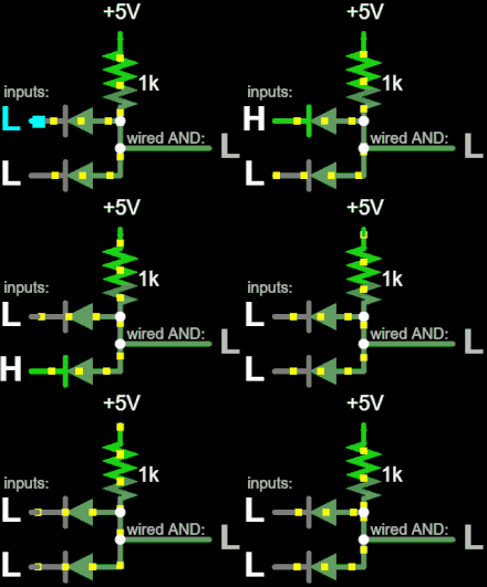
The wired AND connection is a form of AND gate. When using open collector or similar outputs (which can be identified by the ⎐ symbol in schematics), wired AND only requires a pull up resistor on the shared output wire. In this example, 5V is considered HIGH (true), and 0V is LOW (false). This gate can be easily extended with more inputs.
When all inputs are HIGH, they all present high impedance, and the pull-up resistor pulls output voltage HIGH, but if any input is LOW, they pull the output LOW:[1]
| Inputs | Output | |
|---|---|---|
| A | B | A AND B |
| HIGH | LOW | LOW |
| LOW | HIGH | LOW |
| LOW | LOW | LOW |
| HIGH | HIGH | HIGH |
When driving a load, the HIGH output is reduced by the pull-up's voltage drop, though the LOW output is almost 0V. But if diode logic is used, each input requires a diode, and the LOW output voltage will additionally be raised by the diode's forward voltage. Care should be taken to ensure the output still lies within valid voltage levels.
Active-high wired OR connection

See also: Diode logic § Active-high OR logic gate
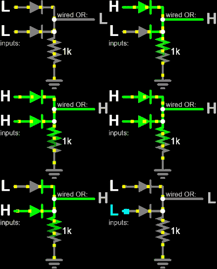
The wired OR connection electrically performs the Boolean logic operation of an OR gate using open emitter or similar inputs (which can be identified by the ⎏ symbol in schematics) connected to a shared output with a pull-down resistor. This gate can also be easily extended with more inputs.
When all inputs are LOW, they all present high impedance, and the pull-down resistor pulls the output voltage LOW, but if any input is HIGH, they pull the output HIGH:
| Inputs | Output | |
|---|---|---|
| A | B | A OR B |
| LOW | LOW | LOW |
| LOW | HIGH | HIGH |
| HIGH | LOW | HIGH |
| HIGH | HIGH | HIGH |
When driving a load, the LOW output is raised by the pull-down's voltage drop, though the HIGH output is almost the supply voltage (5V). But if diode logic is used, each input requires a diode, and the HIGH output voltage will additionally be lowered by the diode's forward voltage.
Reversing active level
An active-high wired AND can be treated as active-low wired OR (and an active-high wired OR can be treated as active-low wired AND), by using active-low logic (or negative logic) and applying De Morgan's laws.
Compatibility of wired AND OR using diodes
Diode logic uses a diode for each input in addition to a shared pull-up resistor (for wired AND) or a pull-down resistor (for wired OR). However, each stage of diode logic reduces output voltage levels. So without amplification, the output voltage may not be compatible with the primary logic family.
References
- M. Morris Mano, Digital Logic and Computer Design, Prentice-Hall, 1979 ISBN 0-13-214510-3, page 571
- Digital Techniques, Heathkit Educational Systems,1990
- Fundamental Physics, K.L Gomber and K.L Gogia,Pradeep Publications, 2005

