Electron diffraction
Electron diffraction refers to the bending of electron beams around atomic structures. This behaviour, typical for waves, is applicable to electrons due to the wave–particle duality stating that electrons behave as both particles and waves. Since the diffracted beams interfere, they generate diffraction patterns widely used for analysis of the objects which caused the diffraction. Therefore, electron diffraction can also refer to derived experimental techniques used for material characterization. This technique is similar to X-ray and neutron diffraction.
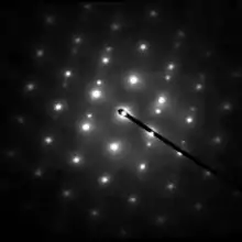
Electron diffraction is most frequently used in solid state physics and chemistry to study crystalline, quasi-crystalline and amorphous materials using electron microscopes. In these instruments, electrons are accelerated by an electrostatic potential in order to gain energy and shorten their wavelength. With the wavelength sufficiently short, the atomic structure acts as a diffraction grating generating diffraction patterns, which carry the information about the crystal orientation, lattice parameters, crystal defects etc.
In transmission electron microscopy (TEM), the most frequent technique related to the electron diffraction is selected area diffraction allowing to measure crystal properties or reconstruct its structure. Despite the technique was considered qualitative for a long time, thanks to modern analytical software it offers quantitative analysis. In scanning electron microscopy (SEM), electron backscatter diffraction is used to determine crystal orientation across the sample. The potential of electron diffraction is not only limited to solids. It can be used to characterize individual molecules dispersed in a gaseous atmosphere using gas electron diffraction.
History
.jpg.webp)
.jpg.webp)
Experiments involving electron beam are dated long before the discovery of electron. In 1650, Otto von Guericke invented vacuum pump[1] allowing the physicists to study effects of high voltage electricity passing through rarefied air. It was noted that electrostatic generator sparks travel a longer distance through low pressure air than through atmospheric pressure air. In 1857, German physicist Heinrich Geissler was able to achieve a pressure of around 10−3 atm and with voltages between a few kilovolts and 100 kV he observed glow discharge. By the 1870s, British physicist William Crookes and others were able to evacuate tubes below 10−6 atm and observed, that the glow in the whole tube disappeared with lowering pressure but the glass behind the anode began to glow. The reason was, that the low pressure allowed the electrons to fly from cathode to the anode without collisions. Even though they were attracted to the anode, they flew so fast, they passed the anode and collided with the tube wall behind making it glow.
The electron beam was discovered in 1869 by German physicist Johann Hittorf.[2] He noticed a shadow cast by the anode on the tube wall behind the anode. He correctly induced that there must be rays emitted from the cathode. Another German scientist Eugen Goldstein named them cathode rays[3] (German kathodenstrahlen). In 1897, Joseph Thomson measured the mass of cathode rays proving they were made of particles. These particles, however, were 1800 times lighter than the lightest particle known by then - a hydrogen atom. Therefore, the first subatomic particle was discovered, originally called corpuscle and later named electron. Thomson also showed electrons were identical with particles given off by photoelectric and radioactive materials.[4]
Paradoxically, Thomson's discovery did not bring the cathode rays and diffraction much closer to each other, since the diffraction was a phenomenon specific to waves, not particles like electrons. The light diffraction was first described already in the 17th century by Italian priest and physicist Francesco Maria Grimaldi.[5] But the light was suggested to be of a wave nature in 1803 when British scientist Thomas Young performed his experiment with two slits.[6] The wave theory was further supported by studies and calculations of French physicist Augustin-Jean Fresnel 1816[7] and 1818[8] finally confirming theory of Christiaan Huygens.[9]
Understanding to the nature of electron beam has fundamentally changed in 1925, when French physicist Louis de Broglie published his hypothesis.[10] He stated that all matter particles can behave as waves and therefore, among other important implications, can be diffracted. The de Broglie hypothesis was experimentally confirmed for electrons in two experiments performed independently by George Paget Thomson[11] and Clinton Joseph Davisson. This sparked a rapid development of electron-based analytical techniques in the 1930s from gas electron diffraction invented by Herman Mark to the first electron microscopes developed by Ernst Ruska.[12]
Theory
Electron interaction with matter
In order to be diffracted, electrons need to interact with matter. Due to their negative electric charge, their interactions differ from other radiation used in diffraction studies of materials such as X-rays and neutrons. Negative electrons are scattered due to Coulomb forces when they interact with a positively charged atomic core. In comparison, X-rays are scattered after interactions with valence electrons, while neutrons are scattered by the atomic nuclei through the strong nuclear force.[13]
Electron diffraction occurs as the result of an elastic scattering, when the incident electrons do not lose their kinetic energy in their interactions with atoms. In some cases, however, even inelastically scattered electrons can be diffracted as the result of a following elastic interaction.
Wavelength of electrons
Due to the wave-particle duality, electrons behave as particles as well as waves. A basic characteristic of the wave is a wavelength. The electron wavelength is given by de Broglie equation as[10]
Here is Planck's constant and [14] is momentum, where is the electron mass and the velocity. Since the electrons are charged particles, they can be accelerated using electric potential. This allows the electrons to get accelerated to speeds, where relativistic theory needs to be applied. Therefore, there are two definitions of wavelength - non-relativistic and relativistic.
Non-relativistic theory
In a non-relativistic theory, the electrons accelerated in an electric potential gain the velocity given by the equation[14]
where is the electron rest mass, is the elementary charge and is the speed of light. Substituting the momentum and velocity to the de Broglie equation we receive
Relativistic theory
| [kV] | [pm] |
|---|---|
| 0.1 | 122.633 |
| 0.5 | 54.832 |
| 1 | 38.763 |
| 10 | 12.204 |
| 20 | 8.588 |
| 50 | 5.355 |
| 100 | 3.701 |
| 200 | 2.508 |
| 300 | 1.969 |
| 400 | 1.644 |
| 800 | 1.027 |
| 1000 | 0.872 |
| 2000 | 0.504 |
| 3000 | 0.357 |
In an electron microscope, the accelerating potential is usually several thousand volts, causing the electron to travel at an appreciable fraction of the speed of light. Scanning electron microscopes typically operate at an accelerating voltage of 10,000 volts (10 kV) giving an electron velocity approximately 20% of the speed of light, while a typical TEM operates at 200 kV raising the electron velocity to 70% the speed of light. Therefore, relativistic effects need to be taken into account. The relativistic relation between energy and momentum is[14]
It follows then, that the ratio between the electron mass and its rest mass (or Lorentz factor) is[14]
Then the relativistic velocity is given by the equation[14]
Substitution of the De Broglie equation to the above expression of energy gives[14]
which leads to the final expression for the relativistic wavelength[14]
The wavelength of the electrons in a 10 kV SEM is then 12.2 × 10⁻¹² m (12.2 pm) while in a 200 kV TEM the wavelength is 2.5 pm. In comparison, the wavelength of X-rays usually used in X-ray diffraction is in the order of 100 pm (Cu Kα: λ=154 pm).
Diffraction on atomic lattice
Wavelength of the electron beam used in a typical electron microscope is sufficiently small, that crystal lattice acts as a diffraction grating. Therefore a diffraction pattern can be formed with beams diffracted under certain angles and intensities.
Diffraction angles

Due to the diffraction, part of the electrons is scattered at particular angles (diffracted beams), while others pass through the sample without changing their direction (transmitted beams). In order to determine the diffraction angles, the electron beam normally incident to the atomic lattice can be seen as a planar wave, which is re-transmitted by each atom as a spherical wave. Due to the constructive interference, the spherical waves from number of diffracted beams under angles given by the equation
where the integer is an order of diffraction and is the distance between atoms if we only assume one row of atoms as shown in the illustration aside. For a real-world 3D atomic structure, it would be an interplanar distance of plane with Miller indices , which needs to be oriented parallel to the electron beam.
Intensity of diffracted beams
In the kinematic theory of diffraction, the intensity of a diffracted beam corresponding to a plane with Miller indices is proportional to sqare of the structure factor, which is defined as
where the sum is over all atoms in the unit cell, are the positional coordinates of the -th atom, and is the atomic scattering factor of the -th atom.[16]
Kinematical theory expects the electron to interact with the matter only once. For many applications, this does not pose significant limitations. For study of more complex diffraction phenomenons, dynamical simulations using for instance Multislice or Bloch waves is needed.[14]
Effect of crystallinity
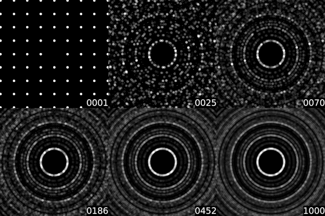
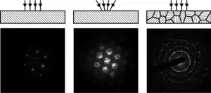
Character of the resulting diffraction pattern depends on whether the beam is diffracted by one single crystal or by number of differently oriented crystallites for instance in a polycrystalline material. The single-crystalline diffractogram depicts a regular pattern of bright spots. This pattern can be seen as a two-dimensional projection of reciprocal crystal lattice. If there are more contributing crystallites, the diffraction image becomes a superposition of individual crystals' diffraction patterns. Ultimately, this superposition contains diffraction spots of all possible crystallographic plane systems in all possible orientations. These conditions result in a diffractogram of concentric rings of discrete radii for the following reasons:
- The discreteness of ring radii is given by the fact, that there are discrete spacings between various parallel crystallographic planes in given crystal system and therefore the beams satisfying the diffraction condition can only form diffraction spots in discrete distances from the transmitted beam.
- The concentricity and ringlike shape is given by the fact, that there are all possible orientations of crystallographic planes and therefore the diffraction spots are formed all around the transmitted beam (rings centre) at the distance (ring radius) corresponding to particular crystalographic plane.
Kikuchi lines
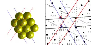
Kikuchi lines are linear diffractogram features created by electrons scattered first inelastically and then elastically. As the electron beam interacts with matter, some electrons are diffracted via elastic scattering, while other can be scattered inelastically losing part of their kinetic energy. Direction of inelastically scattered electrons is significantly less predictive - they can more or less follow the direction of the original beam as well as be "reflected" back. In all cases, they continue to interact with the matter and some of them are diffracted. These electrons then form Kikuchi lines.[17]
Kikuchi lines are paired forming Kikuchi bands. They are indexed after the crystallographic planes they were formed with. Angular width of the band is equal to the diffraction angle specified above which means, that in the diffractogram, the width of plane will be equal to the distance between transmitted beam and diffraction spot. The position of Kikuchi bands is fixed against each other but not against the diffraction spots. As the crystal is tilted in the electron beam, the bands move on the diffraction pattern.[17]
Diffraction by individual molecules in gases
Diffraction can be also performed on individual molecules dispersed in a gaseous atmosphere. Since the beam is dffracted by multiple molecules with all possible orientations relative to the beam, the resulting scattering pattern consists of concentric rings analogously to the diffraction cones produced by polycrystalline materials described above.
In gas electron diffraction (GED) the diffraction intensities at a particular diffraction angle are described via so-called scattering variable defined as
The total intensity is then given as a sum of partial contributions:
where results from scattering by individual atoms, by pairs of atoms and by atom triplets. Intensity corresponds to the background which, unlike the previous contributions, must be determined experimentally. Intensity of atomic scattering is defined as
where , is the distance between the scattering object detector, is the intensity of the primary electron beam and is the scattering amplitude of the i-th atom in the molecular structure in the experiment. is the main contribution and easily obtained for known gas composition.
The most valuable information is carried by the intensity of molecular scattering , as it contains information about the distance between all pairs of atoms in the molecule, whether bonded or not. It is given by formula
where is the distance between two atoms, is the mean square amplitude of vibration between the two atoms, is the anharmonicity constant and is a phase factor which is important for atomic pairs with very different nuclear charges. The summation is performed over all atom pairs. Atomic triplet intensity is negligible in most cases.
Applications
In transmission electron microscope
Electron diffraction in a Transmission electron microscopy (TEM) is a versatile technique allowing to determine a wide range of crystallographic quantities. The versatility of TEM originates from its ability to form the electron beam using complex electron optics. Good control of the beam geometry allows to perform various diffraction techniques enabling to measure the crystal lattice constants, study crystal defects or even to reconstruct an unknown crystal structure.
Even though the diffraction analysis in TEM is a strong analytical tool itself, it can be supported by other tools available in TEM either naturally or as an optional equipment. Among other methods, TEM provides magnified sample image or even high-resolution image, chemical analysis through energy-dispersive X-ray spectroscopy, investigations of electronic structure and bonding through electron energy loss spectroscopy, and studies of the mean inner potential through electron holography.
Compared to another widely used material characterization technique, X-ray diffraction, TEM analysis is significantly more localized. Due to the longer radius of Ewald sphere, electron diffraction also offers constructive interference in a broader diffractogram area resulting in bright diffraction spots in higher distances from the optical axis.
Formation of diffraction image

In TEM, electron beam passes through a thin film of the examined material. Before and after its interaction with the sample, the beam is formed by various elements of electron optics including magnetic lenses, deflectors or apertures. Optical elements above the sample are used to control the incident beam geometry allowing for a wide and parallel beam, focused nanoscopic probe or convergent cone-shaped beam. As it interacts with the sample, part of the beam is diffracted and part is transmitted through the sample without changing its direction.
Below the sample, the beam is deflected by the magnetic lens. Each set of initially parallel rays intersect at certain point in the back focal plane forming a diffraction pattern. The transmitted rays intersect right in the optical axis. The diffracted rays intersect at certain distance from the optical axis (corresponding to interplanar distance of the planes diffracting the beam) and under certain azimuth (corresponding to the orientation of the planes diffracting the beam). In case or parallel incident beam, those intersections can be seen as bright diffraction spots typical for selected area diffraction. In the image plane below the back focal plane, a magnified image of the sample is formed. Further electron optics allows to select which plane is projected to the microscope camera and, therefore, whether a magnified image or diffractogram is acquired. Modern microscopes allow to switch between the imaging and diffraction mode by pressing a single button, which makes diffraction data easily available and accessible.[13]
Wide parallel beam
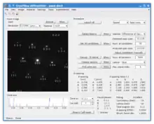
The simplest diffraction technique in TEM is selected area (electron) diffraction (SAED) for which the incident beam is wide and parallel. In order to select particular region of interest from which the diffraction should be received, a selected area aperture is used. It is located right below the sample and can be positioned so that it only allows to pass the wanted portion of the beam blocking the rest. This way, the analysis can be limited for instance to individual crystallites.
If a parallel beam is used to acquire a diffraction pattern from a single-crystal, the resulting image can be seen as a two-dimensional projection of the crystal reciprocal lattice. The depicted diffraction spots correspond to individual crystallographic planes which satisfy diffraction conditions. This allows to determine interplanar distances and angles or crystal symmetry. In combination with modern automated analytical software such as CrysTBox, SAED can be used for a quantitative analysis with picometric precision.[18]
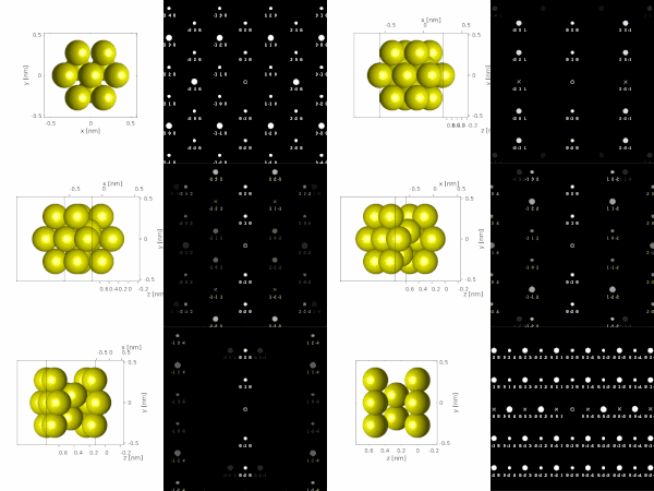
If the sample is tilted against the electron beam, diffraction conditions are satisfied for different set of crystallographic planes yielding different constellation of diffraction spots. This allows to determine the crystal orientation, which can be used for instance to set the orientation needed for particular experiment, to determine misorientation between adjacent grains or crystal twins.[15][18] Since different sample orientations result in different projections of the reciprocal lattice, they provide an opportunity to reconstruct the three-dimensional information about the crystal structure lost in individual projections. A series of diffractograms varying in tilt can be acquired and processed using a diffraction tomography analysis in order to reconstruct an unknown crystal structure.[19]
Kikuchi lines occur in TEM especially in thicker samples, where inelastic scattering followed by the elastic one occurs with sufficient frequency. Since the position of Kikuchi bands within the diffractogram is quite sensitive to crystal orientation, they can be used to fine-tune a zone-axis orientation. Alternatively, they allow to determine crystal orientation with significantly higher accuracy than what is feasible with a spot diffraction analysis. Since mutual positions and orientations of Kikuchi bands is fixed and since the bands intersect in low-index zone axes, they can be used for navigation when changing the orientation between zone axes connected by some band. For those purposes, Kikuchi maps are available.[13]
If the illuminated area selected by the aperture covers many differently oriented crystallites, their diffraction patterns superimpose forming an image of concentric rings. The ring diffractogram is typical for polycrystalline samples, powders or nanoparticles. A diameter of each ring corresponds to interplanar distance of a plane system present in the sample. Instead of information about individual grains or sample orientation, this diffractogram provides more of a statistical information for instance about overall crystallinity or texture. Textured materials can be recognized by a non-uniform distribution of intensity along the ring circumference despite sufficient crystallinity. Ring diffractograms can be also used to discriminate between nanocrystalline and amorphous phases.[15]
Microprobe and nanoprobe
Apart from limiting the beam using the selected area aperture, the site-selectivity can be achieved by condensing the incident beam into a narrow electron probe. This technique is called microprobe or nanoprobe diffraction or simply nanodiffraction. Probes of diameter smaller than 1 nm can be obtained.[13] At these extremes the probe dimension comes at the price of the beam becoming nearly parallel, even though microprobe can be achieved with parallel beam.[15] Compared to SAED, the resulting diffraction spots can be significantly broader and blurry, making a manual analysis quite inaccurate. Accurate processing is possible with automated software like CrysTBox, which is able to take into account a number of diffraction reflections across the whole pattern significantly improving accuracy and repeatability of the analysis.[18]
Convergent beam
In Convergent Beam Electron Diffraction (CBED), the incident electrons are focused in a converging cone-shaped beam with the crossover located in the sample volume. Unlike the parallel beam, the convergent beam is able to carry information from the sample volume, not just a two-dimensional projection available in SAED. With convergent beam there is also no need for the selected area aperture, as it is inherently site-selective since the beam crossover is positioned to the object plane where the sample is located.[17]
A CBED pattern consists of disks arranged exactly the same as the spots in SAED. Intensity within the disks, however, is not uniform, but depicts various features and symmetries reflecting the sample structure. Even though the zone axis and lattice parameter analysis based on disk positions does not significantly differ from SAED, the analysis of disks content is significantly more complex. Due to a number of contributing factors, simulation based on dynamical diffraction theory is often required. With appropriate analysis, however, CBED patterns can be used for indexation of the crystal point group, space group identification, measurement of lattice parameters, thickness or strain.[17]
The disk diameter can be controlled using the beam convergence angle. The larger is the angle, the broader the disks are depicting more features. If the angle is increased to certain level, the disks begin to overlap deteriorating the contained information. This can be solved for instance via a large angle convergent electron beam diffraction (LACBED) where the sample is moved upwards or downwards. There are applications, however, where the overlapping disks are beneficial. Ronchigram could serve as an example. It is a CBED pattern of an amorphous sample depicting many intentionally overlapping disks blended into one image providing information about electron optical system.[13]
In gases
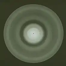
Gas electron diffraction (GED) can be used to determine geometry of molecules dispersed in gases. A gas carrying the examined molecules is exposed to the electron beam, which is diffracted on the molecules. Since the diffracting molecules are randomly oriented, the resulting diffraction pattern consists of concentric rings. The experimentally acquired diffraction intensity is a summation of several components such as background, atomic intensity or molecular intensity.
The most valuable information about the molecular geometry is carried by the molecular intensity , which is specific to pairs of molecular atoms as described above in Theory. If this intensity is derived from an experimental diffractogram by subtracting other contributing intensities, it can be used to match and refine a structural model against the experimental data using an appropriate software.
As an alternative to GED, microwave spectroscopy can be used.
In scanning electron microscope
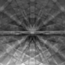
In Scanning electron microscope the sample surface is mapped using a scanning electron beam. The diffraction image is formed using an electron backscatter diffraction (EBSD). A thin layer of the sample material is penetrated by the electrons, some of which are reflected due to the interactions inside the material and are diffracted on their journey out of the sample. As result of the inelastic scattering followed by the elastic one, typical features for an EBSD image are Kikuchi lines. Since the position of Kikuchi bands is highly sensitive to the crystal orientation, EBSD data acquired using the scanning beam can be used to determine the crystal orientation at particular location on the sample surface. The data are processed by an automated software allowing to routinely generate two-dimensional orientation maps across the sample surface. As the Kikuchi lines carry information about the interplanar angles and distances and, therefore, about the crystal structure, they can be also used for a phase identification or strain analysis.[20]
See also
- Diffraction
- Selected area diffraction
- Convergent beam electron diffraction
- Electron backscatter diffraction
- Gas electron diffraction
- Low-energy electron diffraction
- Precession Electron Diffraction
- Reflection high-energy electron diffraction
- Ronchigram
- Kikuchi line
- Electron crystallography
- Electron microscope
- Transmission electron microscopy
- Scanning electron microscopy
- CrysTBox
- Microcrystal electron diffraction
- Diffraction
- Crystal structure
- Stereographic projection
- Zone axis
References
- Harsch, Viktor (November 2007). "Otto von Gericke (1602–1686) and his pioneering vacuum experiments". Aviation, Space, and Environmental Medicine. 78 (11): 1075–1077. doi:10.3357/asem.2159.2007. ISSN 0095-6562. PMID 18018443.
- Martin, Andre (1986), "Cathode Ray Tubes for Industrial and Military Applications", in Hawkes, Peter (ed.), Advances in Electronics and Electron Physics, Volume 67, Academic Press, p. 183, ISBN 9780080577333,
Evidence for the existence of "cathode-rays" was first found by Plücker and Hittorf ...
- E. Goldstein (May 4, 1876) "Vorläufige Mittheilungen über elektrische Entladungen in verdünnten Gasen" (Preliminary communications on electric discharges in rarefied gases), Monatsberichte der Königlich Preussischen Akademie der Wissenschaften zu Berlin (Monthly Reports of the Royal Prussian Academy of Science in Berlin), 279-295. From page 286: "13. Das durch die Kathodenstrahlen in der Wand hervorgerufene Phosphorescenzlicht ist höchst selten von gleichförmiger Intensität auf der von ihm bedeckten Fläche, und zeigt oft sehr barocke Muster." (13. The phosphorescent light that's produced in the wall by the cathode rays is very rarely of uniform intensity on the surface that it covers, and [it] often shows very baroque patterns.)
- Thomson, J. J. (August 1901). "On bodies smaller than atoms". The Popular Science Monthly. Bonnier Corp.: 323–335. Retrieved 2009-06-21.
- Francesco Maria Grimaldi, Physico-mathesis de lumine, coloribus, et iride, aliisque adnexis … [The physical mathematics of light, color, and the rainbow, and other things appended …] (Bologna ("Bonomia"), (Italy): Vittorio Bonati, 1665), pp. 1–11 Archived 2016-12-01 at the Wayback Machine: "Propositio I. Lumen propagatur seu diffunditur non solum directe, refracte, ac reflexe, sed etiam alio quodam quarto modo, diffracte." (Proposition 1. Light propagates or spreads not only in a straight line, by refraction, and by reflection, but also by a somewhat different fourth way: by diffraction.) On p. 187, Grimaldi also discusses the interference of light from two sources: "Propositio XXII. Lumen aliquando per sui communicationem reddit obscuriorem superficiem corporis aliunde, ac prius illustratam." (Proposition 22. Sometimes light, as a result of its transmission, renders dark a body's surface, [which had been] previously illuminated by another [source].)
- "I. The Bakerian Lecture. Experiments and calculations relative to physical optics". Philosophical Transactions of the Royal Society of London. The Royal Society. 94: 1–16. 1804-12-31. doi:10.1098/rstl.1804.0001. ISSN 0261-0523. S2CID 110408369.
- Fresnel, Augustin-Jean (1816), "Mémoire sur la diffraction de la lumière" ("Memoir on the diffraction of light"), Annales de Chimie et de Physique, vol. 1, pp. 239–81 (March 1816); reprinted as "Deuxième Mémoire…" ("Second Memoir…") in Oeuvres complètes d'Augustin Fresnel, vol. 1 (Paris: Imprimerie Impériale, 1866), pp. 89–122. (Revision of the "First Memoir" submitted on 15 October 1815.)
- Fresnel, Augustin-Jean (1818), "Mémoire sur la diffraction de la lumière" ("Memoir on the diffraction of light"), deposited 29 July 1818, "crowned" 15 March 1819, published in Mémoires de l'Académie Royale des Sciences de l'Institut de France, vol. V (for 1821 & 1822, printed 1826), pp. 339–475; reprinted in Oeuvres complètes d'Augustin Fresnel, vol. 1 (Paris: Imprimerie Impériale, 1866), pp. 247–364; partly translated as "Fresnel's prize memoir on the diffraction of light", in H. Crew (ed.), The Wave Theory of Light: Memoirs by Huygens, Young and Fresnel, American Book Company, 1900, pp. 81–144. (First published, as extracts only, in Annales de Chimie et de Physique, vol. 11 (1819), pp. 246–96, 337–78.)
- Christiaan Huygens, Traité de la lumiere … Archived 2016-06-16 at the Wayback Machine (Leiden, Netherlands: Pieter van der Aa, 1690), Chapter 1. From p. 15 Archived 2016-12-01 at the Wayback Machine: "J'ay donc monstré de quelle façon l'on peut concevoir que la lumiere s'etend successivement par des ondes spheriques, … " (I have thus shown in what manner one can imagine that light propagates successively by spherical waves, … ) (Note: Huygens published his Traité in 1690; however, in the preface to his book, Huygens states that in 1678 he first communicated his book to the French Royal Academy of Sciences.)
- De Broglie, Louis (1925). "Recherches sur la théorie des Quanta". Annales de Physique. EDP Sciences. 10 (3): 22–128. Bibcode:1925AnPh...10...22D. doi:10.1051/anphys/192510030022. ISSN 0003-4169.
- Thomson, G. P. (1927). "Diffraction of Cathode Rays by a Thin Film". Nature. 119 (3007): 890. Bibcode:1927Natur.119Q.890T. doi:10.1038/119890a0.
- Ruska, Ernst (1987-08-01). "The development of the electron microscope and of electron microscopy". Bioscience Reports. Portland Press Ltd. 7 (8): 607–629. doi:10.1007/bf01127674. ISSN 0144-8463. PMID 3322421. S2CID 37346966.
- Fultz, B (2013). Transmission electron microscopy and diffractometry of materials. Heidelberg New York: Springer. ISBN 978-3-642-43315-3. OCLC 796932144.
- Kirkland, Earl (2010). Advanced computing in electron microscopy. New York: Springer. ISBN 978-1-4419-6533-2. OCLC 668095602.
- De Graef, Marc (2003-03-27). Introduction to Conventional Transmission Electron Microscopy. Cambridge University Press. doi:10.1017/cbo9780511615092. ISBN 978-0-521-62006-2.
- "Structure Factor". Online Dictionary of CRYSTALLOGRAPHY. IUCr. Retrieved 2022-02-22.
- Morniroli, Jean Paul (2004). Large-Angle Convergent-Beam Electron Diffraction Applications to Crystal Defects. Taylor & Francis. doi:10.1201/9781420034073. ISBN 978-2-901483-05-2.
- Klinger, Miloslav (2017-07-07). "More features, more tools, more CrysTBox". Journal of Applied Crystallography. International Union of Crystallography (IUCr). 50 (4): 1226–1234. doi:10.1107/s1600576717006793. ISSN 1600-5767.
- Gemmi, Mauro; Mugnaioli, Enrico; Gorelik, Tatiana E.; Kolb, Ute; Palatinus, Lukas; Boullay, Philippe; Hovmöller, Sven; Abrahams, Jan Pieter (2019-07-19). "3D Electron Diffraction: The Nanocrystallography Revolution". ACS Central Science. American Chemical Society (ACS). 5 (8): 1315–1329. doi:10.1021/acscentsci.9b00394. ISSN 2374-7943. PMC 6716134. PMID 31482114.
- Schwartz, Adam (2009). Electron backscatter diffraction in materials science. New York, NY: Springer. ISBN 978-0-387-88135-5. OCLC 568751820.
External links
- Virtual lab on electron diffraction
- Jmol-mediated image/diffraction analysis of an unknown
- PTCLab-Program for calculation phase transformation crystallography with diffraction simulation, its free and open source python program https://code.google.com/p/transformation-crystallography-lab/
- ronchigram.com Web simulator for generating convergent beam diffraction of amorphous materials.
