Intel 80188
The Intel 80188 microprocessor was a variant of the Intel 80186. The 80188 had an 8-bit external data bus instead of the 16-bit bus of the 80186; this made it less expensive to connect to peripherals. The 16-bit registers and the one megabyte address range were unchanged, however. It had a throughput of 1 million instructions per second.[5] Intel second sourced this microprocessor to Fujitsu Limited around 1985.[6] Both packages of Intel 80188 version were available in 68-pin PLCC and PGA in sampling at third quarter of 1985.[7] The available 80C188EB in fully static design for the application-specific standard product using the 1-micron CHMOS IV technology. They were available in 3- and 5-Volts version with 84-lead PLCC and 80-lead EIAJ QFP version. It was also available for USD $15.15 in 1,000 unit quantities.[8]
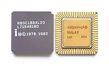
 An Intel R80C188XL20, an LCC variant of the 80188 processor. It has a ceramic heat spreader and gold plated contacts on the bottom. | |
| General information | |
|---|---|
| Launched | 1982 |
| Discontinued | September 2007[1] |
| Common manufacturer(s) | |
| Performance | |
| Max. CPU clock rate | 6 MHz to 40 MHz |
| Data width | 8 bits |
| Address width | 20 bits |
| Architecture and classification | |
| Technology node | 3 µm[3] to 1 µm[4] |
| Instruction set | x86-16 |
| Physical specifications | |
| Transistors |
|
| Cores |
|
| Co-processor | Intel 80187 |
| Package(s) | |
| Socket(s) | |
| Products, models, variants | |
| Variant(s) |
|
| History | |
| Predecessor(s) | Intel 8088 |
| Successor(s) | Intel 80386 (The 80286 was also introduced in early 1982, and thus contemporary with the 80186) |
Description
Features and performance
The 80188 series was generally intended for embedded systems, as microcontrollers with external memory. Therefore, to reduce the number of chips required, it included features such as clock generator, interrupt controller, timers, wait state generator, DMA channels, and external chip select lines. While the N80188 was compatible with the 8087 numeric co-processor, the 80C188 was not. It did not have the ESC control codes integrated.
The initial clock rate of the 80188 was 6 MHz, but due to more hardware available for the microcode to use, especially for address calculation, many individual instructions ran faster than on an 8086 at the same clock frequency. For instance, the common register+immediate[lower-alpha 1] addressing mode was significantly faster than on the 8086, especially when a memory location was both (one of the) operand(s) and the destination. Multiply and divide also showed great improvement, being several times as fast as on the original 8086 and multi-bit shifts were done almost four times as quickly as in the 8086.
End of life
Along with hundreds of other processor models, Intel discontinued the 80188 processor 30 March 2006, after a life of about 24 years.[9]
Notes
- In fact, all variants, including reg+reg and reg+reg+immediate were faster.
References
- "Product Change Notification" (PDF). 2 May 2006. Archived from the original (PDF) on 9 October 2006.
- "Intel 80188 family". CPU World.
- "3 µm lithography process". WikiChip.
- Intel Corporation, "New Product Focus: Components: New ASSP Suits Mobile Applications", Microcomputer Solutions, September/October 1990, page 11
- Pacheco, Alberto (2001-10-12). "1.3 La familia de microprocesadores de Intel" [Intel Processors: MCS-4, MCS-8, MCS-85, x86: IA-16, IA-32, IA-64.]. CB-00-852/01. Lenguaje Ensamblador (in English and Spanish). Instituto Tecnológico de Chihuahua. Archived from the original on April 24, 2012. Retrieved July 20, 2010.
- Intel Corporation, "NewsBits: Second Source News", Solutions, January/February 1985, Page 1
- Ashborn, Jim; "Advanced Packaging: A Little Goes A Long Way", Intel Corporation, Solutions, January/February 1986, Page 2
- Intel Corporation, "New Product Focus: Components: New ASSP Suits Mobile Applications", Microcomputer Solutions, September/October 1990, page 11
- "Product Change Notification 106013 - 01" (PDF). Intel. May 2, 2006. Archived from the original (PDF) on October 9, 2006.
External links
- Intel 80186/80188 images and descriptions at cpu-collection.de
- Scan of the Intel 80188 data book at datasheetarchive.com