Sunny Cove (microarchitecture)
Sunny Cove is a codename for a CPU microarchitecture developed by Intel, first released in September 2019. It succeeds the Palm Cove microarchitecture and is fabricated using Intel's 10 nm process node.[1] The microarchitecture is implemented in 10th-generation Intel Core processors for mobile (codenamed Ice Lake) and third generation Xeon scalable server processors (codenamed Ice Lake-SP). 10th-generation Intel Core mobile processors were released in September 2019, while the Xeon server processors were released on April 6, 2021.[2]
| General information | |
|---|---|
| Launched | September 2019 |
| Designed by | Intel |
| Common manufacturer(s) | |
| Cache | |
| L1 cache | 80 KB per core:
|
| L2 cache | 512 KB per core |
| L3 cache | 2 MB per core |
| Architecture and classification | |
| Technology node | Intel 10 nm FinFET process |
| Instruction set | x86, x86-64 |
| Extensions | |
| Products, models, variants | |
| Product code name(s) |
|
| History | |
| Predecessor(s) | |
| Successor(s) |
|
There are no desktop products featuring Sunny Cove. However, a variant named Cypress Cove is used for the 11th-generation Intel Core desktop processors (codenamed Rocket Lake). Cypress Cove is a version of the Sunny Cove microarchitecture backported to Intel's 14 nm process node.[3]
The direct successor to the Sunny Cove microarchitecture is the Willow Cove microarchitecture, which powers the 11th-generation Intel Core mobile processors.[4]
Features
Sunny Cove was designed by Intel Israel's processor design team in Haifa, Israel.[5][6]
Intel released details of Ice Lake and its microarchitecture, Sunny Cove, during Intel Architecture Day in December 2018, stating that the Sunny Cove cores would be focusing on single-thread performance, new instructions, and scalability improvements. Intel stated that the performance improvements would be achieved by making the core "deeper, wider, and smarter".[7]
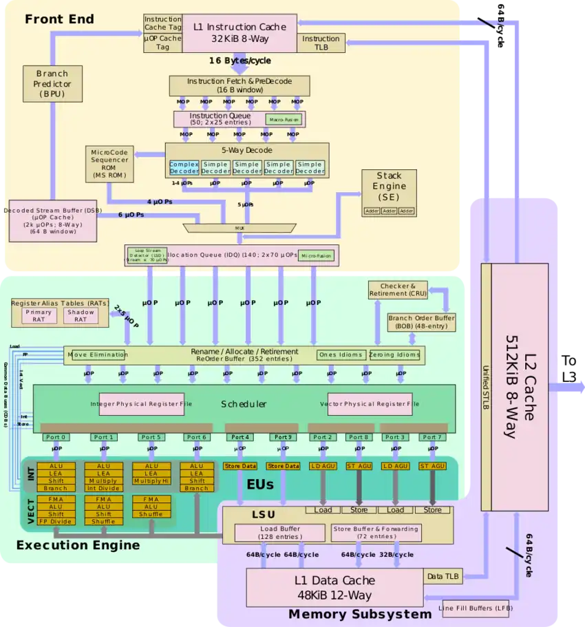
Sunny Cove features a 50% increase in the size of L1 data cache, a larger L2 cache dependent on product size, larger μOP cache, and larger second-level TLB. The core has also increased in width, by increasing execution ports from eight to ten and by doubling the L1 store bandwidth. Allocation width has also increased from four to five. The 5-level paging scheme supports a linear address space up to 57 bits and a physical address space up to 52 bits, increasing the virtual memory space to 128 petabytes, up from 256 terabytes, and the addressable physical memory to 4 petabytes, up from 64 terabytes.[8][7]
Improvements
- On average 18% increase in IPC in comparison to 2015 Skylake running at the same frequency and memory configuration[9][10]
- Increase L1 data cache: 48 kiB (from 32 kiB)
- L2 cache: 512 kiB[11]
- Larger micro-instruction cache (2304 entries, up from 1536)
- Larger re-order buffer (352, up from 224 entries)
- Dynamic Tuning 2.0 which allows the CPU to stay at turbo frequencies for longer[12][13]
- Hardware acceleration for SHA operations (Secure Hash Algorithms)
- New AVX-512 instruction subsets:
- Wider decoder (from skylake's 3 simple + 1 complex 4 way decoding to Sunny cove's 4 simple + 1 complex 5 wide decoder)
- 1.6x larger ROB (352, up from 224 entries)
- Scheduler
- 1.65x larger scheduler (160-entry, up from 97 entries)
- Larger dispatch (10-way, up from 8-way)
- 1.55x larger integer register file (280-entry, up from 180)
- 1.33x larger vector register file (224-entry, up from 168)
- Distributed scheduling queues (4 scheduling queues, up from 2)
- Scheduler
- Intel Deep Learning Boost, used for machine learning/artificial intelligence inference acceleration[14][13]
Cypress Cove
 Cypress Cove die from an i5-11400 | |
| General information | |
|---|---|
| Launched | March 30, 2021 |
| Designed by | Intel |
| Common manufacturer(s) | |
| Cache | |
| L1 cache | 80 KB per core:
|
| L2 cache | 512 KB per core |
| L3 cache | 2 MB per core |
| Architecture and classification | |
| Technology node | Intel 14 nm FinFET process |
| Instruction set | x86, x86-64 |
| Extensions | |
| Products, models, variants | |
| Product code name(s) | |
| History | |
| Predecessor(s) | Skylake |
| Successor(s) | Golden Cove |
Cypress Cove is a CPU microarchitecture based on the Sunny Cove microarchitecture designed for 10 nm, backported to 14 nm. It succeeds the Skylake microarchitecture, and is manufactured using Intel's 14 nm process node. Cypress Cove is identical to Sunny Cove, aside from a number of improvements and other changes.[15] Notably the L1 data cache latency has been reduced from five cycles that is on Sunny Cove to just three cycles on Cypress Cove. Intel claims an increase of 19% in IPC in Cypress Cove-based Rocket Lake processors compared to Comet Lake.[15][16]
Cypress Cove is implemented on 11th Gen Intel Core desktop processors (codenamed Rocket Lake). Rocket Lake and its underlying microarchitecture were first described in November 2020,[3] and was later released on March 30, 2021.[17][18]
SGX is removed from Rocket Lake.
Products
Sunny Cove powers the 10th generation of Intel Core mobile processors (codenamed Ice Lake) and the third generation of Xeon Scalable server processors (codenamed Ice Lake-SP). Cypress Cove is implemented on 11th-generation Intel Core desktop processors (codenamed Rocket Lake).
References
- Garreffa, Anthony (January 21, 2016). "Intel teases its Ice Lake & Tiger Lake family, 10nm for 2018 and 2019". TweakTown. Retrieved June 3, 2016.
- "Media Alert: Intel to Launch 3rd Gen Intel Xeon Scalable Portfolio". Intel Newsroom. Santa Clara, CA. March 22, 2021. Retrieved April 9, 2021.
- Cutress, Ian (October 29, 2020). "Intel's 11th Gen Core Rocket Lake Detailed: Ice Lake Core with Xe Graphics". AnandTech. Retrieved April 6, 2021.
- Cutress, Ian (August 13, 2020). "Intel's 11th Gen Core Tiger Lake SoC Detailed: SuperFin, Willow Cove and Xe-LP". AnandTech. Retrieved September 29, 2020.
- "Intel launches 10th gen core processor developed in Israel". en.globes.co.il (in Hebrew). May 28, 2019. Retrieved October 6, 2019.
- Solomon, Shoshanna (May 28, 2019). "Intel launches new processors that bring AI to the PC, sired by Haifa team". The Times of Israel. Retrieved October 6, 2019.
- Cutress, Ian (December 12, 2018). "Intel's Architecture Day 2018: The Future of Core, Intel GPUs, 10nm, and Hybrid x86". AnandTech. Retrieved January 14, 2019.
- "5-Level Paging and 5-Level EPT" (PDF). Intel. May 2017.
- Schor, David (May 28, 2019). "Intel Sunny Cove Core To Deliver A Major Improvement In Single-Thread Performance, Bigger Improvements To Follow". WikiChip Fuse. Retrieved May 28, 2019.
- Schor, David (May 28, 2019). "Intel Announces 10th Gen Core Processors Based On 10nm Ice Lake, Now Shipping". WikiChip Fuse. Retrieved May 28, 2019.
- "Intel Ice Lake 10nm CPU Benchmark Leak Shows More Cache, Higher Performance". HotHardware. HotHardware. October 23, 2018. Retrieved November 9, 2018.
{{cite news}}: CS1 maint: others (link) - "Dynamic Tuning - Intel - WikiChip". WikiChip. Retrieved May 28, 2019.
- Cutress, Ian (July 30, 2019). "Examining Intel's Ice Lake Processors: Taking a Bite of the Sunny Cove Microarchitecture". AnandTech. Retrieved August 1, 2019.
- "Intel® Deep Learning Boost". Intel AI. Retrieved August 1, 2019.
- Cutress, Ian (March 30, 2021). "Intel Rocket Lake (14nm) Review: Core i9-11900K, Core i7-11700K, and Core i5-11600K". AnandTech. Retrieved April 6, 2021.
- "11th Gen Intel Core: Unmatched Overclocking, Game Performance". Intel Newsroom. March 15, 2021. Retrieved April 6, 2021.
- Alcorn, Paul (March 23, 2021). "Intel Rocket Lake Price, Benchmarks, Specs and Release Date, All We Know". Tom's Hardware. Retrieved April 6, 2021.
- Mah Ung, Gordon (March 16, 2021). "Intel's new 11th-gen Rocket Lake-S CPU: Everything you need to know". PCWorld. Retrieved April 6, 2021.
