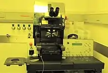
Aligner (semiconductor)
An aligner, or mask aligner, is a system that produces integrated circuits (IC) using the photolithography process. It holds the photomask over the silicon wafer while a bright light is shone through the mask and onto the photoresist. The "alignment" refers to the ability to place the mask over precisely the same location repeatedly as the chip goes through multiple rounds of lithography. Aligners were a major part of IC manufacture from the 1960s into the late 1970s, when they began to be replaced by the stepper.[1][2]

There are several distinct generations of aligner technology. The early contact aligners placed the mask in direct contact with the top surface of the wafer, which often damaged the pattern when the mask was lifted off again. Used only briefly, proximity aligners held the mask slightly above the surface to avoid this problem, but were difficult to work with and required considerable manual adjustment. Finally, the Micralign projection aligner, introduced by Perkin-Elmer in 1973, held the mask entirely separate from the chip and made the adjustment of the image much simpler.[1][2] Through these stages of development, yields improved from perhaps 10% to about 70%, leading to a corresponding reduction in chip prices.[1][2]
The stepper is similar to an aligner in concept, but with one key difference. The aligner uses a mask that holds the pattern for the entire wafer, which may require large masks. The stepper uses a mask on the wafer repeatedly, and steps across the surface to repeat the pattern of the chip layer. This reduces mask costs dramatically and allows a single wafer to be used for different mask designs in a single run. More importantly, by focussing the light source onto a single area of the wafer, the stepper can produce much higher resolutions, thus allowing for smaller features on chips (minimum feature size). The disadvantage to the stepper is that each chip on the wafer has to be individually imaged, and thus the process of exposing the wafer as a whole is much slower.
References
- International directory of company histories. Vol. 7. Paula Kepos, Thomson Gale. Detroit, Mich.: St. James Press. 1993. ISBN 978-1-55862-648-5. OCLC 769042405.
{{cite book}}: CS1 maint: others (link) - "History of The Perkin-Elmer Corporation – FundingUniverse". www.fundinguniverse.com. Archived from the original on February 4, 2013. Retrieved 2022-12-25.
External links
- Burbank, Daniel (Fall 1999). "The Near Impossibility of Making a Microchip" (PDF). Invention & Technology.