Common source
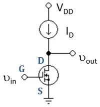
In electronics, a common-source amplifier is one of three basic single-stage field-effect transistor (FET) amplifier topologies, typically used as a voltage or transconductance amplifier. The easiest way to tell if a FET is common source, common drain, or common gate is to examine where the signal enters and leaves. The remaining terminal is what is known as "common". In this example, the signal enters the gate, and exits the drain. The only terminal remaining is the source. This is a common-source FET circuit. The analogous bipolar junction transistor circuit may be viewed as a transconductance amplifier or as a voltage amplifier. (See classification of amplifiers). As a transconductance amplifier, the input voltage is seen as modulating the current going to the load. As a voltage amplifier, input voltage modulates the current flowing through the FET, changing the voltage across the output resistance according to Ohm's law. However, the FET device's output resistance typically is not high enough for a reasonable transconductance amplifier (ideally infinite), nor low enough for a decent voltage amplifier (ideally zero). As seen below in the formula, the voltage gain depends on the load resistance, so it cannot be applied to drive low-resistance devices, such as a speaker (having a resistance of 8 ohms). Another major drawback is the amplifier's limited high-frequency response. Therefore, in practice the output often is routed through either a voltage follower (common-drain or CD stage), or a current follower (common-gate or CG stage), to obtain more favorable output and frequency characteristics. The CS–CG combination is called a cascode amplifier.


Characteristics
At low frequencies and using a simplified hybrid-pi model (where the output resistance due to channel length modulation is not considered), the following closed-loop small-signal characteristics can be derived.
| Definition | Expression | |
|---|---|---|
| Current gain | ||
| Voltage gain | ||
| Input impedance | ||
| Output impedance |
Bandwidth


Bandwidth of common-source amplifier tends to be low, due to high capacitance resulting from the Miller effect. The gate-drain capacitance is effectively multiplied by the factor , thus increasing the total input capacitance and lowering the overall bandwidth.
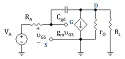
Figure 3 shows a MOSFET common-source amplifier with an active load. Figure 4 shows the corresponding small-signal circuit when a load resistor RL is added at the output node and a Thévenin driver of applied voltage VA and series resistance RA is added at the input node. The limitation on bandwidth in this circuit stems from the coupling of parasitic transistor capacitance Cgd between gate and drain and the series resistance of the source RA. (There are other parasitic capacitances, but they are neglected here as they have only a secondary effect on bandwidth.)
Using Miller's theorem, the circuit of Figure 4 is transformed to that of Figure 5, which shows the Miller capacitance CM on the input side of the circuit. The size of CM is decided by equating the current in the input circuit of Figure 5 through the Miller capacitance, say iM, which is:
- ,
to the current drawn from the input by capacitor Cgd in Figure 4, namely jωCgd vGD. These two currents are the same, making the two circuits have the same input behavior, provided the Miller capacitance is given by:
- .
Usually the frequency dependence of the gain vD / vG is unimportant for frequencies even somewhat above the corner frequency of the amplifier, which means a low-frequency hybrid-pi model is accurate for determining vD / vG. This evaluation is Miller's approximation[1] and provides the estimate (just set the capacitances to zero in Figure 5):
- ,
so the Miller capacitance is
- .
The gain gm (rO || RL) is large for large RL, so even a small parasitic capacitance Cgd can become a large influence in the frequency response of the amplifier, and many circuit tricks are used to counteract this effect. One trick is to add a common-gate (current-follower) stage to make a cascode circuit. The current-follower stage presents a load to the common-source stage that is very small, namely the input resistance of the current follower (RL ≈ 1 / gm ≈ Vov / (2ID) ; see common gate). Small RL reduces CM.[2] The article on the common-emitter amplifier discusses other solutions to this problem.
Returning to Figure 5, the gate voltage is related to the input signal by voltage division as:
- .
The bandwidth (also called the 3 dB frequency) is the frequency where the signal drops to 1/ √2 of its low-frequency value. (In decibels, dB(√2) = 3.01 dB). A reduction to 1/ √2 occurs when ωCM RA = 1, making the input signal at this value of ω (call this value ω3 dB, say) vG = VA / (1+j). The magnitude of (1+j) = √2. As a result, the 3 dB frequency f3 dB = ω3 dB / (2π) is:
- .
If the parasitic gate-to-source capacitance Cgs is included in the analysis, it simply is parallel with CM, so
- .
Notice that f3 dB becomes large if the source resistance RA is small, so the Miller amplification of the capacitance has little effect upon the bandwidth for small RA. This observation suggests another circuit trick to increase bandwidth: add a common-drain (voltage-follower) stage between the driver and the common-source stage so the Thévenin resistance of the combined driver plus voltage follower is less than the RA of the original driver.[3]
Examination of the output side of the circuit in Figure 2 enables the frequency dependence of the gain vD / vG to be found, providing a check that the low-frequency evaluation of the Miller capacitance is adequate for frequencies f even larger than f3 dB. (See article on pole splitting to see how the output side of the circuit is handled.)
See also
References
- R.R. Spencer; M.S. Ghausi (2003). Introduction to electronic circuit design. Upper Saddle River NJ: Prentice Hall/Pearson Education, Inc. p. 533. ISBN 0-201-36183-3.
- Thomas H Lee (2004). The design of CMOS radio-frequency integrated circuits (Second ed.). Cambridge UK: Cambridge University Press. pp. 246–248. ISBN 0-521-83539-9.
- Thomas H Lee (2004). pp. 251–252. ISBN 0-521-83539-9.
_8.6.10.1.b.svg.png.webp)
_8.6.1.svg.png.webp)