Control register
A control register is a processor register that changes or controls the general behavior of a CPU or other digital device. Common tasks performed by control registers include interrupt control, switching the addressing mode, paging control, and coprocessor control.
History
When IBM developed a paging version[note 1] of the System/360, they added 16 control registers[1][2] to the design for what became the 360/67. IBM did not provide control registers on other S/360 models, but made them a standard part[3] of System/370, although with different register and bit assignments. As IBM added new features to the architecture, e.g., DAS, S/370-XA, S/370-ESA, ESA/390, they added additional fields to the control registers. With z/Architecture, IBM doubled the control register size to 64 bits.
Control registers in IBM 360/67
On the 360/67, CR0 and CR2 are used by address translation, CR 4-6 contain miscellaneous flags including interrupt masks and Extended Control Mode,[2] and CR 8-14[4] contain the switch settings on the 2167 Configuration Unit.
M67 CR0
Control Register 0 contains the address of the segment table for dynamic address translation.
M67 CR2
Control register 2 is the Relocation exception address register.
M67 CR4
CR4 is the extended mask register for channels 0-31. Each bit is the 1/0 channel mask for the corresponding channel.
M67 CR5
CR5 is reserved for the extended mask register for channels 32–63. Each bit is the 1/0 channel mask for the corresponding channel.
M67 CR6
CR6 contains two mode flags plus extensions to the PSW mask bits.
| Field | Bit | Description |
|---|---|---|
| 0 | 0 | Machine Check Mask Extension for Channel Controller o |
| 1 | 1 | Machine Check Mask Extension for Channel Controller 1 |
| 2-3 | Reserved for channel controllers 2-3 | |
| 4-7 | Unassigned | |
| 8 | 8 | Extended Control Mode |
| 9 | 9 | Configuration Control Bit |
| 10-23 | Unassigned | |
| 24-31 | External interrupt masking | |
| 24 | Timer | |
| 25 | Interrupt Key | |
| 26 | Malfunction Alert - CPU 1 (Ext. Sig. 2) | |
| 27 | Malfunction Alert - CPU 2 (Ext. Sig. 3) | |
| 28 | Reserved (Ext. Sig. 4) | |
| 29 | Reserved (Ext. Sig. 5) | |
| 30 | External Interrupt - CPU 1, 2 (Ext. Sig. 6) | |
| 31 | Reserved (Ext. Sig. 7) |
M67 CR8
Control Register 8 contains the assignments of Processor Storage units 1–4 to central processing units (CPUs) and channel controllers (CCs).
| Bit | Description |
|---|---|
| 0 | Processor Storage Unit 1 to CPU 1 |
| 1 | Processor Storage Unit 1 to CPU 2 |
| 2-3 | Reserved for CPU 3-4 |
| 4 | Processor Storage Unit 1 to CC 0 |
| 5 | Processor Storage Unit 1 to CC 1 |
| 6-7 | Reserved for CC 3-4 |
| 8 | Processor Storage Unit 2 to CPU 1 |
| 9 | Processor Storage Unit 2 to CPU 2 |
| 10-11 | Reserved for CPU 3-4 |
| 12 | Processor Storage Unit 2 to CC 0 |
| 13 | Processor Storage Unit 2 to CC 1 |
| 14-15 | Reserved for CC 3-4 |
| 16 | Processor Storage Unit 3 to CPU 1 |
| 17 | Processor Storage Unit 3 to CPU 2 |
| 18-19 | Reserved for CPU 3-4 |
| 20 | Processor Storage Unit 3 to CC 0 |
| 21 | Processor Storage Unit 3 to CC 1 |
| 22-23 | Reserved for CC 3-4 |
| 24 | Processor Storage Unit 4 to CPU 1 |
| 25 | Processor Storage Unit 4 to CPU 2 |
| 26-27 | Reserved for CPU 3-4 |
| 28 | Processor Storage Unit 4 to CC 0 |
| 29 | Processor Storage Unit 4 to CC 1 |
| 30-31 | Reserved for CC 3-4 |
M67 CR9
Control Register 9 contains the assignments of Processor Storage units 5–8 to central processing units (CPUs) and channel controllers (CCs).
| Bit | Description |
|---|---|
| 0 | Processor Storage Unit 5 to CPU 1 |
| 1 | Processor Storage Unit 5 to CPU 2 |
| 2-3 | Reserved for CPU 3-4 |
| 4 | Processor Storage Unit 5 to CC 0 |
| 5 | Processor Storage Unit 5 to CC 1 |
| 6-7 | Reserved for CC 3-4 |
| 8 | Processor Storage Unit 6 to CPU 66 |
| 9 | Processor Storage Unit 6 to CPU 2 |
| 10-11 | Reserved for CPU 3-4 |
| 12 | Processor Storage Unit 6 to CC 0 |
| 13 | Processor Storage Unit 6 to CC 1 |
| 14-15 | Reserved for CC 3-4 |
| 16 | Processor Storage Unit 7 to CPU 1 |
| 17 | Processor Storage Unit 7 to CPU 2 |
| 18-19 | Reserved for CPU 3-4 |
| 20 | Processor Storage Unit 7 to CC 0 |
| 21 | Processor Storage Unit 7 to CC 1 |
| 22-23 | Reserved for CC 3-4 |
| 24 | Processor Storage Unit 8 to CPU 1 |
| 25 | Processor Storage Unit 8 to CPU 2 |
| 26-27 | Reserved for CPU 3-4 |
| 28 | Processor Storage Unit 8 to CC 0 |
| 29 | Processor Storage Unit 8 to CC 1 |
| 30-31 | Reserved for CC 3-4 |
M67 CR10
Control Register 10 contains the Processor storage address assignment codes.
| Bit | Starting Address Code for |
|---|---|
| 0-3 | Processor Storage Unit 1 |
| 4-7 | Processor Storage Unit 2 |
| 8-11 | Processor Storage Unit 3 |
| 12-15 | Processor Storage Unit 4 |
| 16-19 | Processor Storage Unit 5 |
| 20-23 | Processor Storage Unit 6 |
| 24-27 | Processor Storage Unit 7 |
| 28-31 | Processor Storage Unit 8 |
M67 CR11
Control Register 11 contains channel controller (CC) assignments.
| Bit | Description |
|---|---|
| 0 | CC 0 available on CPU 1 |
| 1 | CC 0 available on CPU 2 |
| 2-3 | Reserved for CPUs 3-4 |
| 4 | CC 1 available on CPU 1 |
| 5 | CC 1 available on CPU 2 |
| 6-7 | Reserved for CPUs 3-4 |
| 8-15 | Unassigned |
| 16 | CPU 1 to only CC 0 |
| 17 | CPU 1 to only CC 1 |
| 18-19 | Reserved for CC 2-3 |
| 20 | CPU 2 to only CC 0 |
| 21 | CPU 2 to only CC 1 |
| 22-23 | Reserved for CC 2-3 |
| 24-31 | Unassigned |
M67 CR12
CR12 contains I/O Control Unit Partitioning.
| Bit | I/O Control Unit | Interface |
|---|---|---|
| 0 | 1 | 1 |
| 1 | 2 | |
| 2 | 2 | 1 |
| 3 | 2 | |
| 4 | 3 | 1 |
| 5 | 2 | |
| 6 | 4 | 1 |
| 7 | 2 | |
| 8 | 5 | 1 |
| 9 | 2 | |
| 10 | 6 | 1 |
| 11 | 2 | |
| 12 | 7 | 1 |
| 13 | 2 | |
| 14 | 8 | 1 |
| 15 | 2 | |
| 16 | 9 | 1 |
| 17 | 2 | |
| 18 | 10 | 1 |
| 19 | 2 | |
| 20 | 11 | 1 |
| 21 | 2 | |
| 22 | 12 | 1 |
| 23 | 2 | |
| 24 | 13 | 1 |
| 25 | 2 | |
| 26 | 14 | 1 |
| 27 | 2 | |
| 28 | 15 | 1 |
| 29 | 2 | |
| 30 | 16 | 1 |
| 31 | 2 |
M67 CR13
CR13 contains I/O Control Unit Partitioning.
| Bit | I/O Control Unit | Interface |
|---|---|---|
| 0 | 17 | 1 |
| 1 | 2 | |
| 2 | 18 | 1 |
| 3 | 2 | |
| 4 | 19 | 1 |
| 5 | 2 | |
| 6 | 20 | 1 |
| 7 | 2 | |
| 8 | 21 | 1 |
| 9 | 2 | |
| 10 | 22 | 1 |
| 11 | 2 | |
| 12 | 23 | 1 |
| 13 | 2 | |
| 14 | 24 | 1 |
| 15 | 2 | |
| 16 | 25 | 1 |
| 17 | 2 | |
| 18 | 26 | 1 |
| 19 | 2 | |
| 20 | 27 | 1 |
| 21 | 2 | |
| 22 | 28 | 1 |
| 23 | 2 | |
| 24 | 29 | 1 |
| 25 | 2 | |
| 26 | 30 | 1 |
| 27 | 2 | |
| 28 | 31 | 1 |
| 29 | 2 | |
| 30 | 32 | 1 |
| 31 | 2 |
M67 CR14
CR14 contains indicators.
| Bit | Indicator |
|---|---|
| 0-27 | Unassigned |
| 22 | 2167 Power On |
| 23 | Unassigned |
| 24 | Direct Control, CPU 1 |
| 25 | Direct Control, CPU 2 |
| 26-27 | Unassigned |
| 28 | Prefix, CPU 1 |
| 29 | Prefix, CPU 2 |
| 30-31 | Unassigned |
Control registers in IBM S/390
The control registers of ESA/390[5] on the IBM S/390 are an evolutionary enhancement to the control registers on the earlier ESA/370,[6] S/370-XA[7] and S/370[8] processors. For details on which fields are dependent on specific features, consult the Principles of Operation.[9]
| CR | bits | Field |
|---|---|---|
| 0 | 1 | SSM-suppression |
| 0 | 2 | TOD-clock-sync control |
| 0 | 3 | Low-address-protection control |
| 0 | 4 | Extraction-authority control |
| 0 | 5 | Secondary-space control |
| 0 | 6 | Fetch-protection-override control |
| 0 | 7 | Storage-protection-override control |
| 0 | 8-12 | Translation format |
| 0 | 13 | AFP-register control |
| 0 | 14 | Vector control |
| 0 | 15 | Address-space-function control |
| 0 | 16 | Malfunction-alert subclass mask |
| 0 | 17 | Emergency-signal subclass mask |
| 0 | 18 | External-call subclass mask |
| 0 | 19 | TOD-clock sync-check subclass mask |
| 0 | 20 | Clock-comparator subclass mask |
| 0 | 21 | CPU-timer subclass mask |
| 0 | 22 | Service-signal subclass mask |
| 0 | 24 | Set to 1 |
| 0 | 25 | Interrupt-key subclass mask |
| 0 | 26 | Set to 1 |
| 0 | 27 | ETR subclass mask |
| 0 | 28 | Program-call-fast |
| 0 | 29 | Crypto control |
| 1 | 0 | Primary space-switch-event control |
| 1 | 1-19 | Primary segment-table origin |
| 1 | 22 | Primary subspace-group control |
| 1 | 23 | Primary private-space control |
| 1 | 24 | Primary storage-alteration-event control |
| 1 | 25-31 | Primary segment-table length |
| 2 | 1-25 | Dispatchable-unit-control-table origin |
| 3 | 0-15 | PSW-key mask |
| 3 | 16-31 | Secondary ASN |
| 4 | 0-15 | Authorization index |
| 4 | 16-31 | Primary ASN |
| 5 | 0 | Subsystem-linkage control |
| 5 | 1-24 | Linkage-table origin |
| 5 | 25-31 | Linkage-table length |
| 5 | 1-25 | When the address-space-function control is one, Primary-ASN-second-table-entry |
| 6 | 0-7 | I/O-interruption subclass mask |
| 7 | 1-19 | Secondary segment-table origin |
| 7 | 22 | Secondary subspace-group control |
| 7 | 23 | Secondary private-space control |
| 7 | 24 | Secondary storage-alteration-event control |
| 7 | 25-31 | Secondary segment-table length |
| 8 | 0-15 | Extended authorization index |
| 8 | 16-31 | Monitor masks |
| 9 | 0 | Successful-branching-event mask |
| 9 | 1 | Instruction-fetching-event mask |
| 9 | 2 | Storage-alteration-event mask |
| 9 | 3 | GR-alteration-event mask |
| 9 | 4 | Store-using-real-address-event mask |
| 9 | 8 | Branch-address control |
| 9 | 10 | Storage-alteration-space control |
| 9 | 16-31 | PER general-register masks |
| 10 | 1-31 | PER starting address |
| 11 | 1-31 | PER ending address |
| 12 | 0 | Branch-trace control |
| 12 | 1-29 | Trace-entry address |
| 12 | 30 | ASN-trace control |
| 12 | 31 | Explicit-trace control |
| 13 | 0 | Home space-switch-event control |
| 13 | 1-19 | Home segment-table origin |
| 13 | 23 | Home private-space control |
| 13 | 24 | Home storage-alteration-event control |
| 13 | 25-31 | Home segment-table length |
| 14 | 0 | Set to 1 |
| 14 | 1 | Set to 1 |
| 14 | 2 | Extended-save-area control |
| 14 | 3 | Channel-report-pending subclass mask |
| 14 | 4 | Recovery subclass mask |
| 14 | 5 | Degradation subclass mask |
| 14 | 6 | External-damage subclass mask |
| 14 | 7 | Warning subclass mask |
| 14 | 10 | TOD-clock-control-override control |
| 14 | 12 | ASN-translation control |
| 14 | 13-31 | ASN-first-table origin |
| 15 | 1-28 | Linkage-stack-entry address |
Control registers in Intel x86 series
CR0
The CR0 register is 32 bits long on the 386 and higher processors. On x64 processors in long mode, it (and the other control registers) is 64 bits long. CR0 has various control flags that modify the basic operation of the processor. Register CR0 is the 32 Bit version of the old Machine Status Word (MSW) register. The MSW register was expanded to the Control Register with the appearance of the i386 processor.
| Bit | Name | Full Name | Description |
|---|---|---|---|
| 0 | PE | Protected Mode Enable | If 1, system is in protected mode, else, system is in real mode |
| 1 | MP | Monitor co-processor | Controls interaction of WAIT/FWAIT instructions with TS flag in CR0 |
| 2 | EM | Emulation | If set, no x87 floating-point unit present, if clear, x87 FPU present |
| 3 | TS | Task switched | Allows saving x87 task context upon a task switch only after x87 instruction used |
| 4 | ET | Extension type | On the 386, it allowed to specify whether the external math coprocessor was an 80287 or 80387 |
| 5 | NE | Numeric error | Enable internal x87 floating point error reporting when set, else enables PC style x87 error detection |
| 16 | WP | Write protect | When set, the CPU can't write to read-only pages when privilege level is 0 |
| 18 | AM | Alignment mask | Alignment check enabled if AM set, AC flag (in EFLAGS register) set, and privilege level is 3 |
| 29 | NW | Not-write through | Globally enables/disable write-through caching |
| 30 | CD | Cache disable | Globally enables/disable the memory cache |
| 31 | PG | Paging | If 1, enable paging and use the § CR3 register, else disable paging. |
CR1
Reserved, the CPU will throw a #UD exception when trying to access it.
CR2
Contains a value called Page Fault Linear Address (PFLA). When a page fault occurs, the address the program attempted to access is stored in the CR2 register.
CR3
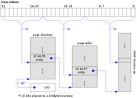
Used when virtual addressing is enabled, hence when the PG bit is set in CR0. CR3 enables the processor to translate linear addresses into physical addresses by locating the page directory and page tables for the current task. Typically, the upper 20 bits of CR3 become the page directory base register (PDBR), which stores the physical address of the first page directory. If the PCIDE bit in CR4 is set, the lowest 12 bits are used for the process-context identifier (PCID).[10]
CR4
Used in protected mode to control operations such as virtual-8086 support, enabling I/O breakpoints, page size extension and machine-check exceptions.
| Bit | Name | Full Name | Description |
|---|---|---|---|
| 0 | VME | Virtual 8086 Mode Extensions | If set, enables support for the virtual interrupt flag (VIF) in virtual-8086 mode. |
| 1 | PVI | Protected-mode Virtual Interrupts | If set, enables support for the virtual interrupt flag (VIF) in protected mode. |
| 2 | TSD | Time Stamp Disable | If set, RDTSC instruction can only be executed when in ring 0, otherwise RDTSC can be used at any privilege level. |
| 3 | DE | Debugging Extensions | If set, enables debug register based breaks on I/O space access. |
| 4 | PSE | Page Size Extension | If set, enables 32-bit paging mode to use 4 MiB huge pages in addition to 4 KiB pages.
If PAE is enabled or the processor is in x86-64 long mode this bit is ignored.[11] |
| 5 | PAE | Physical Address Extension | If set, changes page table layout to translate 32-bit virtual addresses into extended 36-bit physical addresses. |
| 6 | MCE | Machine Check Exception | If set, enables machine check interrupts to occur. |
| 7 | PGE | Page Global Enabled | If set, address translations (PDE or PTE records) may be shared between address spaces. |
| 8 | PCE | Performance-Monitoring Counter enable | If set, RDPMC can be executed at any privilege level, else RDPMC can only be used in ring 0. |
| 9 | OSFXSR | Operating system support for FXSAVE and FXRSTOR instructions | If set, enables Streaming SIMD Extensions (SSE) instructions and fast FPU save & restore. |
| 10 | OSXMMEXCPT | Operating System Support for Unmasked SIMD Floating-Point Exceptions | If set, enables unmasked SSE exceptions. |
| 11 | UMIP | User-Mode Instruction Prevention | If set, the SGDT, SIDT, SLDT, SMSW and STR instructions cannot be executed if CPL > 0.[10] |
| 12 | LA57 | 57-Bit Linear Addresses | If set, enables 5-Level Paging.[12][13]: 2–18 |
| 13 | VMXE | Virtual Machine Extensions Enable | see Intel VT-x x86 virtualization. |
| 14 | SMXE | Safer Mode Extensions Enable | see Trusted Execution Technology (TXT) |
| 15 | [lower-alpha 1] | (Reserved) | — |
| 16 | FSGSBASE | FSGSBASE Enable | If set, enables the instructions RDFSBASE, RDGSBASE, WRFSBASE, and WRGSBASE. |
| 17 | PCIDE | PCID Enable | If set, enables process-context identifiers (PCIDs). |
| 18 | OSXSAVE | XSAVE and Processor Extended States Enable | |
| 19 | KL | Key Locker Enable | If set, enables the AES Key Locker instructions. |
| 20 | SMEP[16] | Supervisor Mode Execution Protection Enable | If set, execution of code in a higher ring generates a fault. |
| 21 | SMAP | Supervisor Mode Access Prevention Enable | If set, access of data in a higher ring generates a fault.[17] |
| 22 | PKE | Protection Key Enable | See Intel 64 and IA-32 Architectures Software Developer's Manual. |
| 23 | CET | Control-flow Enforcement Technology | If set, enables control-flow enforcement technology.[13]: 2–19 |
| 24 | PKS | Enable Protection Keys for Supervisor-Mode Pages | If set, each supervisor-mode linear address is associated with a protection key when 4-level or 5-level paging is in use.[13]: 2–19 |
| 25 | UINTR | User Interrupts Enable | If set, enables user-mode inter-processor interrupts and their associated instructions and data structures. |
| 63-26 | — | (Reserved) | — |
CR5–7
Reserved, same case as CR1.
Additional Control registers in Intel x86-64 series
EFER
Extended Feature Enable Register (EFER) is a model-specific register added in the AMD K6 processor, to allow enabling the SYSCALL/SYSRET instruction, and later for entering and exiting long mode. This register becomes architectural in AMD64 and has been adopted by Intel as IA32_EFER. Its MSR number is 0xC0000080.
| Bit | Purpose |
|---|---|
| 0 | SCE (System Call Extensions) |
| 1 | DPE (AMD K6 only: Data Prefetch Enable) |
| 2 | SEWBED (AMD K6 only: Speculative EWBE# Disable) |
| 3 | GEWBED (AMD K6 only: Global EWBE# Disable) |
| 4 | L2D (AMD K6 only: L2 Cache Disable) |
| 5-7 | Reserved, Read as Zero |
| 8 | LME (Long Mode Enable) |
| 9 | Reserved |
| 10 | LMA (Long Mode Active) |
| 11 | NXE (No-Execute Enable) |
| 12 | SVME (Secure Virtual Machine Enable) |
| 13 | LMSLE (Long Mode Segment Limit Enable) |
| 14 | FFXSR (Fast FXSAVE/FXRSTOR) |
| 15 | TCE (Translation Cache Extension) |
| 16 | Reserved |
| 17 | MCOMMIT (MCOMMIT instruction enable) |
| 18 | INTWB (Interruptible WBINVD/WBNOINVD enable) |
| 19 | Reserved |
| 20 | UAIE (Upper Address Ignore Enable) |
| 21 | AIBRSE (Automatic IBRS Enable) |
| 22–63 | Reserved |
CR8
CR8 is a new register accessible in 64-bit mode using the REX prefix. CR8 is used to prioritize external interrupts and is referred to as the task-priority register (TPR).[11]
The AMD64 architecture allows software to define up to 15 external interrupt-priority classes. Priority classes are numbered from 1 to 15, with priority-class 1 being the lowest and priority-class 15 the highest. CR8 uses the four low-order bits for specifying a task priority and the remaining 60 bits are reserved and must be written with zeros.
System software can use the TPR register to temporarily block low-priority interrupts from interrupting a high-priority task. This is accomplished by loading TPR with a value corresponding to the highest-priority interrupt that is to be blocked. For example, loading TPR with a value of 9 (1001b) blocks all interrupts with a priority class of 9 or less, while allowing all interrupts with a priority class of 10 or more to be recognized. Loading TPR with 0 enables all external interrupts. Loading TPR with 15 (1111b) disables all external interrupts.
The TPR is cleared to 0 on reset.
XCR0 and XSS
XCR0, or Extended Control Register 0, is a control register which is used to toggle the storing or loading of registers related to specific CPU features using the XSAVE/XRSTOR instructions. It is also used with some features to enable or disable the processor's ability to execute their corresponding instructions. It can be changed using the privileged XSETBV read using the unprivileged XGETBV instructions.[18]
| Bit | Purpose |
|---|---|
| 0 | X87 (x87 FPU/MMX State, note, must be '1') |
| 1 | SSE (XSAVE feature set enable for MXCSR and XMM regs) |
| 2 | AVX (AVX enable, and XSAVE feature set can be used to manage YMM regs) |
| 3 | BNDREG (MPX enable, and XSAVE feature set can be used for BND regs) |
| 4 | BNDCSR (MPX enable, and XSAVE feature set can be used for BNDCFGU and BNDSTATUS regs) |
| 5 | opmask (AVX-512 enable, and XSAVE feature set can be used for AVX opmask, AKA k-mask, regs) |
| 6 | ZMM_hi256 (AVX-512 enable, and XSAVE feature set can be used for upper-halves of the lower ZMM regs) |
| 7 | Hi16_ZMM (AVX-512 enable, and XSAVE feature set can be used for the upper ZMM regs) |
| 8 | PT (Processor Trace) |
| 9 | PKRU (XSAVE feature set can be used for PKRU register, which is part of the protection keys mechanism) |
| 10 | PASID |
| 11 | CET_U |
| 12 | CET_S |
| 13 | HDC (Hardware duty cycling) |
| 14 | UINTR (User interrupts) |
| 15 | LBR (Last branch record) |
| 16 | HWP (Hardware P-states) |
| 17 | AMX TILECFG |
| 18 | AMX TILEDATA |
| 19 | APX extended GPRs (R16 through R31) |
| 20–63 | Reserved |
There is also the IA32_XSS MSR, which is located at address DA0h. The IA32_XSS MSR controls bits of XCR0 which are considered to be "supervisor" state, and should be invisible to regular programs. It operates with the privileged XSAVES and XRSTORS instructions by adding supervisor state to the data they operate with. Put simply, if the X87 state was enabled in XCR0 and PT state was enabled in IA32_XSS, the XSAVE instruction would only store X87 state, while the privileged XSAVES would store both X87 and PT states. Because it is an MSR, it can be accessed using the RDMSR and WRMSR instructions.
| Bit | Purpose |
|---|---|
| 0–7 | Reserved; must be 0. |
| 8 | PT (Enables the saving and loading of nine Processor Trace MSRs.) |
| 10 | Processor Address Space ID (PASID) state |
| 11 | Control-flow Enforcement Technology (CET) User State |
| 12 | Control-flow Enforcement Technology (CET) Supervisor State |
| 13 | HDC (Enables the saving and loading of the IA32_PM_CTL1 MSR.) |
| 14 | User interrupts (UINTR) state |
| 15 | Last branch recording (LBR) state |
| 16 | HWP (enables the saving/loading of IA32_HWP_REQUEST MSR) |
| 17–63 | Reserved; must be 0. |
See also
Notes
- IBM never shipped the 360/64 or 360/66, only the 360/67.
References
- IBM manuals
- M67prelim
- System/360 Model 67 - Time Sharing System - Preliminary Technical Summary (PDF). C20-1647-0. Retrieved May 8, 2023.
{{cite book}}:|work=ignored (help) - M67
- IBM System/360 Model 67 - Functional Characteristics (PDF). February 1972. A27-2719-0. Retrieved May 8, 2023.
{{cite book}}:|work=ignored (help) - S/370
- IBM System/370 - Principles of Operation (PDF) (Eleventh ed.). IBM. September 1987. GA22-7000-10. Retrieved May 8, 2023.
- S/370-XA
- IBM System/370 Extended Architecture Principles of Operation (PDF) (Second ed.). IBM. January 1987. SA22-7085-1. Retrieved May 8, 2023.
- S/370-ESA
- IBM Enterprise Systems Architecture/370 Principles of Operation (PDF) (First ed.). IBM. August 1988. SA22-7200-0. Retrieved May 8, 2023.
- S/390-ESA
- IBM Enterprise Systems Architecture/390 Principles of Operation (PDF) (Ninth ed.). IBM. June 2003. SA22-7201-08. Retrieved May 8, 2023.
- z/Architecture
- z/Architecture - Principles of Operation (PDF) (Fourteenth ed.). IBM. May 2022. SA22-7832-13. Retrieved May 8, 2023.
- M67prelim, pp. 25-26, Control Registers.
- M67, p. 16, Table 4. Control Registers.
- S/370, pp. 4-8-4-11 , Control Registers.
- M67, pp. 31-35, Control Register Bit Assignments for Sensing.
- S/390-ESA.
- S/370-ESA.
- S/370-XA.
- S/370.
- S/390-ESA, pp. 4-6-4-10, Control Registers.
- Intel Corporation (2016). "4.10.1 Process-Context Identifiers (PCIDs)". Intel 64 and IA-32 Architectures Software Developer's Manual (PDF). Vol. 3A: System Programming Guide, Part 1.
- "AMD64 Architecture Programmer's Manual Volume 2: System Programming" (PDF). AMD. September 2012. pp. 127 & 130. Retrieved 2017-08-04.
- "5-Level Paging and 5-Level EPT" (PDF). Intel. May 2017. p. 16. Retrieved 2018-01-23.
- "Intel 64 and IA-32 Architectures Software Developer's Manual" (PDF). Intel® Corporation. 2021-06-28. Retrieved 2021-09-21.
- Intel, Software Guard Extensions Programming Reference, ref no. 329298-001, sep 2013 - chapters 1.7 and 6.5.2 describe CR4.SEE.
- Intel, Software Guard Extensions Programming Reference, ref no. 329298-002, oct 2014 - makes no mention of CR4.SEE.
- Fischer, Stephen (2011-09-21). "Supervisor Mode Execution Protection" (PDF). NSA Trusted Computing Conference 2011. National Conference Services, Inc. Archived from the original (PDF) on 2016-08-03. Retrieved 2017-08-04.
- Anvin, H. Peter (2012-09-21). "x86: Supervisor Mode Access Prevention". LWN.net. Retrieved 2017-08-04.
- "Chapter 13, Managing State Using The Xsave Feature Set" (PDF). Intel(R) 64 and IA-32 Architectures Software Developer's Manual, Volume 1: Basic Architecture. Intel Corporation (2019). Retrieved 23 March 2019.