Northbridge (computing)
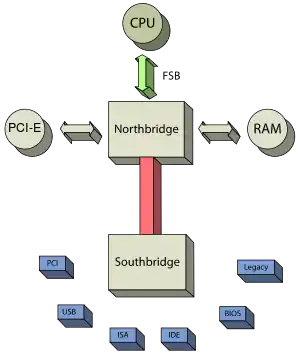
In computing, a northbridge (also host bridge, or memory controller hub) is one of two chips comprising the core logic chipset architecture on a PC motherboard. A northbridge is connected directly to a CPU via the front-side bus (FSB) to handle high-performance tasks, and is usually used in conjunction with a slower southbridge[1] to manage communication between the CPU and other parts of the motherboard.[2] Since the 2010s, die shrink and improved transistor density have allowed for increasing chipset integration, and the functions performed by northbridges are now often incorporated into other components (like southbridges or CPUs themselves).[3][4] As of 2019, Intel and AMD had both released chipsets in which all northbridge functions had been integrated into the CPU.[4] Modern Intel Core processors have the northbridge integrated on the CPU die, where it is known as the uncore or system agent.


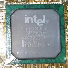
On older Intel based PCs, the northbridge was also named external memory controller hub (MCH) or graphics and memory controller hub (GMCH) if equipped with integrated graphics. Increasingly these functions became integrated into the CPU chip itself,[3] beginning with memory and graphics controllers. For Intel Sandy Bridge and AMD Accelerated Processing Unit processors introduced in 2011, all of the functions of the northbridge reside on the CPU.[5] The corresponding southbridge was renamed by Intel as the Platform Controller Hub and by AMD as the Fusion controller hub. AMD FX CPUs continued to require external northbridge and southbridge chips.
Historically, separation of functions between CPU, northbridge, and southbridge chips was necessary due to the difficulty of integrating all components onto a single chip die.[6] However, as CPU speeds increased over time, a bottleneck emerged due to limitations caused by data transmission between the CPU and its support chipset.[7] The trend for integrated northbridges began near the end of the 2000s — for example, the Nvidia GeForce 320M GPU in the 2010 MacBook Air was a northbridge/southbridge/GPU combo chip.[8]
Overview
The northbridge typically handles communications among the CPU, in some cases RAM, and PCI Express (or AGP) video cards, and the southbridge.[9][10] Some northbridges also contain integrated video controllers, also known as a Graphics and Memory Controller Hub (GMCH) in Intel systems. Because different processors and RAM require different signaling, a given northbridge will typically work with only one or two classes of CPUs and generally only one type of RAM.
There are a few chipsets that support two types of RAM; generally, these are made available when there is a shift to a new standard. For example, the northbridge from the 2002 Nvidia nForce2 chipset only worked with Socket A processors combined with DDR SDRAM.
The Intel i875 chipset will only work with systems using Pentium 4 processors or Celeron processors that have a clock speed greater than 1.3 GHz and utilize DDR SDRAM, and the Intel i915G chipset only works with the Intel Pentium 4 and the Celeron, but it can use DDR or DDR2 memory.
Etymology
The name is derived from drawing the architecture in the fashion of a map. The CPU would be at the top of the map comparable to due north on most general purpose geographical maps. The CPU would be connected to the chipset via a fast bridge (the northbridge) located north of other system devices as drawn. The northbridge would then be connected to the rest of the chipset via a slow bridge (the southbridge) located south of other system devices as drawn.

Overclocking
The northbridge plays an important part in how far a computer can be overclocked, as its frequency is commonly used as a baseline for the CPU to establish its own operating frequency. This chip typically gets hotter as processor speed becomes faster, requiring more cooling. There is a limit to CPU overclocking, as digital circuits are limited by physical factors such as rise, fall, delay and storage times of the transistors, current gain bandwidth product, parasitic capacitance, and propagation delay, which increases with (among other factors) operating temperature; consequently most overclocking applications have software-imposed limits on the multiplier and external clock setting. Additionally, heat is a major limiting factor, as higher voltages are needed to properly activate field effect transistors inside CPUs and this higher voltage produces larger amounts of heat, requiring greater thermal solutions on the die.
Evolution

The overall trend in processor design has been to integrate more functions onto fewer components, which decreases overall motherboard cost and improves performance. The memory controller, which handles communication between the CPU and RAM, was moved onto the processor die by AMD beginning with their AMD K8 processors and by Intel with their Nehalem processors. One of the advantages of having the memory controller integrated on the CPU die is to reduce latency from the CPU to memory.
Another example of this kind of change is Nvidia's nForce3 for AMD K8 systems. It combines all of the features of a normal southbridge with an Accelerated Graphics Port (AGP) port and connects directly to the CPU. On nForce4 boards it was marketed as a media communications processor (MCP).
AMD Accelerated Processing Unit processors feature full integration of northbridge functions onto the CPU chip, along with processor cores, memory controller, high speed PCI Express interface (usually for graphics card), and integrated graphics processing unit (iGPU). This was an evolution of the AMD K8, since the memory controller was integrated on the CPU die in the AMD64.
The northbridge was replaced by the system agent introduced by the Intel Sandy Bridge microarchitecture in 2011, which essentially handles all previous Northbridge functions.[11] Intel's Sandy Bridge processors feature full integration of northbridge functions onto the CPU chip, along with processor cores, memory controller, high speed PCI Express interface and integrated graphics processing unit (GPU). This was a further evolution of the Westmere architecture, which also featured a CPU and GPU in the same package.[12]
Recent AMD processors starting with the Zen 2 have moved some I/O functions out of the CPU die onto an I/O die on the same MCM package as the CPU. This die is not normally considered to be part of the Northbridge, since it is in the same package as the CPU, but it serves some of the same functions.[13]
See also
References
- "Southbridge". TechTarget. Retrieved January 4, 2016.
- "Definition of:Northbridge". PC Magazine. Retrieved September 26, 2015.
- "Trustworthy x86 laptops? There is a way, says system-level security ace". The Register. Retrieved January 4, 2016.
- "Northbridge". Computer Hope. October 7, 2019.
- "Intel i7 2600K (Sandy Bridge) Review". Overclockers.com. 2011-01-03. Retrieved 2015-05-07.
- "Chipset: Northbridge and Southbridge". Rigacci.org. 2006-01-27. Retrieved 2015-05-07.
- Kent, Allen (1999). Encyclopedia of computer science and technology. New York, NY [u.a.]: Dekker. p. 500. ISBN 9780824722937. Retrieved September 26, 2015.
- The Macbook Air: A Sign of Things to Come – Digital Gravitas
- Jones, George (2004-10-22). "Motherboards & Core-Logic Chipsets: The Deep Stuff | What the North Bridge and South Bridge Do". InformIT.com. Retrieved 2015-05-07.
- George Jones - Maximum PC 2005 Buyer's Guide - Prentice Hall PTR - ISBN 0-7686-6312-1
- "The Ring Bus & System Agent - Intel's Sandy Bridge Architecture Exposed". Anandtech.com. Retrieved 2015-05-07.
- "Intel Core i5 2500K and Core i7 2600K (Sandy Bridge) - Introduction". Legionhardware.com. Archived from the original on 2016-06-05. Retrieved 2015-05-07.
- "Chiplets Are the Future, but They Won't Replace Moore's Law".