Ball grid array
A ball grid array (BGA) is a type of surface-mount packaging (a chip carrier) used for integrated circuits. BGA packages are used to permanently mount devices such as microprocessors. A BGA can provide more interconnection pins than can be put on a dual in-line or flat package. The whole bottom surface of the device can be used, instead of just the perimeter. The traces connecting the package's leads to the wires or balls which connect the die to package are also on average shorter than with a perimeter-only type, leading to better performance at high speeds.
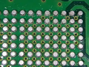
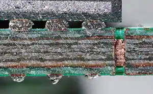
BGAs were introduced in the 1990s and became popular by 2001.[1]
Soldering of BGA devices requires precise control and is usually done by automated processes such as in computer-controlled automatic reflow ovens.
Description
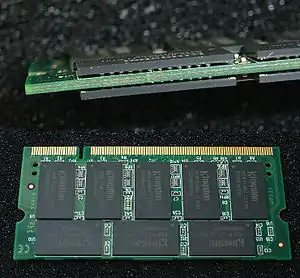
The BGA is descended from the pin grid array (PGA), which is a package with one face covered (or partly covered) with pins in a grid pattern which, in operation, conduct electrical signals between the integrated circuit and the printed circuit board (PCB) on which it is placed. In a BGA the pins are replaced by pads on the bottom of the package, each initially with a tiny solder ball stuck to it. These solder spheres can be placed manually or by automated equipment, and are held in place with a tacky flux.[2] The device is placed on a PCB with copper pads in a pattern that matches the solder balls. The assembly is then heated, either in a reflow oven or by an infrared heater, melting the balls. Surface tension causes the molten solder to hold the package in alignment with the circuit board, at the correct separation distance, while the solder cools and solidifies, forming soldered connections between the device and the PCB.
In more advanced technologies, solder balls may be used on both the PCB and the package. Also, in stacked multi-chip modules, (package on package) solder balls are used to connect two packages.
Advantages
High density
The BGA is a solution to the problem of producing a miniature package for an integrated circuit with many hundreds of pins. Pin grid arrays and dual-in-line surface mount (SOIC) packages were being produced with more and more pins, and with decreasing spacing between the pins, but this was causing difficulties for the soldering process. As package pins got closer together, the danger of accidentally bridging adjacent pins with solder grew.
Heat conduction
A further advantage of BGA packages over packages with discrete leads (i.e. packages with legs) is the lower thermal resistance between the package and the PCB. This allows heat generated by the integrated circuit inside the package to flow more easily to the PCB, preventing the chip from overheating.
Low-inductance leads
The shorter an electrical conductor, the lower its unwanted inductance, a property which causes unwanted distortion of signals in high-speed electronic circuits. BGAs, with their very short distance between the package and the PCB, have low lead inductances, giving them superior electrical performance to pinned devices.
Disadvantages
Lack of compliance
A disadvantage of BGAs is that the solder balls cannot flex in the way that longer leads can, so they are not mechanically compliant. As with all surface mount devices, bending due to a difference in coefficient of thermal expansion between PCB substrate and BGA (thermal stress) or flexing and vibration (mechanical stress) can cause the solder joints to fracture.
Thermal expansion issues can be overcome by matching the mechanical and thermal characteristics of the PCB to those of the package. Typically, plastic BGA devices more closely match PCB thermal characteristics than ceramic devices.
The predominant use of RoHS compliant lead-free solder alloy assemblies has presented some further challenges to BGAs including "head in pillow"[3] soldering phenomenon, "pad cratering" problems as well as their decreased reliability versus lead-based solder BGAs in extreme operating conditions such as high temperature, high thermal shock and high gravitational force environments, in part due to lower ductility of RoHS-compliant solders.[4]
Mechanical stress issues can be overcome by bonding the devices to the board through a process called "underfilling",[5] which injects an epoxy mixture under the device after it is soldered to the PCB, effectively gluing the BGA device to the PCB. There are several types of underfill materials in use with differing properties relative to workability and thermal transfer. An additional advantage of underfill is that it limits tin whisker growth.
Another solution to non-compliant connections is to put a "compliant layer" in the package that allows the balls to physically move in relation to the package. This technique has become standard for packaging DRAMs in BGA packages.
Other techniques for increasing the board-level reliability of packages include use of low-expansion PCBs for ceramic BGA (CBGA) packages, interposers between the package and PCB, and re-packaging a device.[5]
Difficulty of inspection
Once the package is soldered into place, it is difficult to find soldering faults. X-ray machines, industrial CT scanning machines,[6] special microscopes, and endoscopes to look underneath the soldered package have been developed to overcome this problem. If a BGA is found to be badly soldered, it can be removed in a rework station, which is a jig fitted with infrared lamp (or hot air), a thermocouple and a vacuum device for lifting the package. The BGA can be replaced with a new one, or it can be refurbished (or reballed) and re-installed on the circuit board. Pre-configured solder balls matching the array pattern can be used to reball BGAs when only one or a few need to be reworked. For higher volume and repeated lab work, a stencil-configured vacuum-head pick-up and placement of loose spheres can be used.
Due to the cost of visual X-ray BGA inspection, electrical testing is very often used instead. Very common is boundary scan testing using an IEEE 1149.1 JTAG port.
A cheaper and easier inspection method, albeit destructive, is becoming increasingly popular because it does not require special equipment. Commonly referred to as dye and pry, the process includes immersing the entire PCB or just the BGA attached module into a dye, and after drying, the module is pried off and the broken joins are inspected. If a solder location contains the dye, then it indicates that the connection was imperfect.[7]
Difficulties during circuit development
During development it is not practical to solder BGAs into place, and sockets are used instead, but tend to be unreliable. There are two common types of socket: the more reliable type has spring pins that push up under the balls, although it does not allow using BGAs with the balls removed as the spring pins may be too short.
The less reliable type is a ZIF socket, with spring pinchers that grab the balls. This does not work well, especially if the balls are small.
Cost of equipment
Expensive equipment is required to reliably solder BGA packages; hand-soldering BGA packages is very difficult and unreliable, usable only for the smallest packages in the smallest quantities.[8] However, as more ICs have become available only in leadless (e.g. quad-flat no-leads package) or BGA packages, various DIY reflow methods have been developed using inexpensive heat sources such as heat guns, and domestic toaster ovens and electric skillets.[9]
Variants
.jpg.webp)
- CABGA: chip array ball grid array
- CBGA and PBGA denote the ceramic or plastic substrate material to which the array is attached.
- CTBGA: thin chip array ball grid array
- CVBGA: very thin chip array ball grid array
- DSBGA: die-size ball grid array
- FBGA: fine ball grid array based on ball grid array technology. It has thinner contacts and is mainly used in system-on-a-chip designs;
also known as fine pitch ball grid array (JEDEC-Standard[10]) or
fine line BGA by Altera. Not to be confused with fortified BGA.[11] - FCmBGA: flip chip molded ball grid array
- LBGA: low-profile ball grid array
- LFBGA: low-profile fine-pitch ball grid array
- MBGA: micro ball grid array
- MCM-PBGA: multi-chip module plastic ball grid array
- nFBGA: New Fine Ball Grid Array
- PBGA: plastic ball grid array
- SuperBGA (SBGA): super ball grid array
- TABGA: tape array BGA
- TBGA: thin BGA
- TEPBGA: thermally enhanced plastic ball grid array
- TFBGA or thin and fine ball grid array
- UFBGA and UBGA and ultra fine ball grid array based on pitch ball grid array.
- VFBGA: very fine pitch ball grid array
- WFBGA: very very thin profile fine pitch ball grid array
Effectively also the flip chip methods for mounting chip dies to a carrier is sort of a BGA design derivate with the functional equivalent of the balls there being called bumps or micro bumps. This is realized at an already microscopic size level.
To make it easier to use ball grid array devices, most BGA packages only have balls in the outer rings of the package, leaving the innermost square empty.
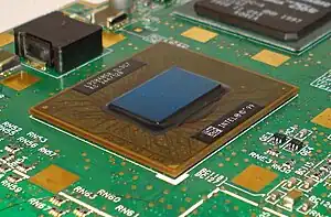
Intel used a package designated BGA1 for their Pentium II and early Celeron mobile processors. BGA2 is Intel's package for their Pentium III and some later Celeron mobile processors. BGA2 is also known as FCBGA-479. It replaced its predecessor, BGA1.
For example, the "micro-FCBGA" (flip chip ball grid array) is Intel's current BGA mounting method for mobile processors that use a flip chip binding technology. It was introduced with the Coppermine Mobile Celeron. Micro-FCBGA has 479 balls that are 0.78 mm in diameter. The processor is affixed to the motherboard by soldering the balls to the motherboard. This is thinner than a pin grid array socket arrangement, but is not removable.
The 479 balls of the Micro-FCBGA package (a package almost identical to the 478-pin socketable micro-FCPGA package) are arranged as the 6 outer rings of a 1.27 mm pitch (20 balls per inch pitch) 26x26 square grid, with the inner 14x14 region empty.[12][13]
Procurement
Primary end-users of BGAs are original equipment manufacturers (OEMs). There is also a market among electronic hobbyists do it yourself (DIY) such as the increasingly popular maker movement.[14] While OEMs generally source their components from the manufacturer, or the manufacturer's distributor, the hobbyist will typically obtain BGAs on the aftermarket through electronic component brokers or distributors.
See also
- Dual in-line package (DIP)
- Pin grid array (PGA)
- Land grid array (LGA)
- Thin quad flat pack (TQFP)
- Small-outline integrated circuit (SOIC)
- Chip carrier: chip packaging and package types list
- Embedded wafer level ball grid array
References
- "Ball Grid Array (BGA) - Engineering Technical - PCBway".
- "Soldering 101 - A Basic Overview". Archived from the original on 2012-03-03. Retrieved 2010-12-29.
- Alpha (2010-03-15) [September 2009]. "Reducing Head in Pillow Defects - Head in pillow defects: causes and potential solutions". 3. Archived from the original on 2013-12-03. Retrieved 2018-06-18.
- "TEERM - TEERM Active Project - NASA-DOD Lead-Free Electronics (Project 2)". Teerm.nasa.gov. Archived from the original on 2014-10-08. Retrieved 2014-03-21.
- Solid State Technology: BGA underfills - Increasing board-level solder joint reliability, 12/01/2001
- "CT Services - Overview." Jesse Garant & Associates. August 17, 2010. "Industrial Computed Tomography Scanning Services – JG&A". Archived from the original on 2010-09-23. Retrieved 2010-11-24.
- "Dye and Pry of BGA Solder Joints" (PDF). cascade-eng.com. 2013-11-22. Archived from the original (PDF) on 2011-10-16. Retrieved 2014-03-22.
- Das, Santosh (2019-08-22). "BGA Soldering & Repairing / How to Solder Ball Grid Array". Electronics and You. Retrieved 2021-09-07.
- Sparkfun tutorials: Reflow skillet, July 2006
- Design Requirements - Fine Pitch Ball Grid Array Package (FBGA) DR-4.27D, jedec.org, MAR 2017
- Ryan J. Leng. "The Secrets of PC Memory: Part 2". 2007.
- Intel. "Mobile Intel Celeron Processor (0.13 μ) in Micro-FCBGA and Micro-FCPGA Packages". Datasheet Archived 2014-03-18 at the Wayback Machine. 2002.
- "FCBGA-479 (Micro-FCBGA)". Archived from the original on 2021-02-28. Retrieved 2011-12-20.
- "More than just digital quilting: The "maker" movement could change how science is taught and boost innovation. It may even herald a new industrial revolution". The Economist. Dec 3, 2011.
External links
- PBGA Package Information from Amkor Technology
- PBGA Package Information Archived 2019-01-02 at the Wayback Machine from J-Devices Corporation