Ion track
Ion tracks are damage-trails created by swift heavy ions penetrating through solids, which may be sufficiently-contiguous for chemical etching in a variety of crystalline, glassy, and/or polymeric solids.[1][2] They are associated with cylindrical damage-regions several nanometers in diameter[3][4] and can be studied by Rutherford backscattering spectrometry (RBS), transmission electron microscopy (TEM), small-angle neutron scattering (SANS), small-angle X-ray scattering (SAXS) or gas permeation.[5]
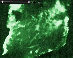
Ion track technology
Ion track technology deals with the production and application of ion tracks in microtechnology and nanotechnology.[6] Ion tracks can be selectively etched in many insulating solids, leading to cones or cylinders, down to 8 nanometers in diameter.[7] Etched track cylinders can be used as filters,[8][9] Coulter counter microchannels,[10] be modified with monolayers,[11] or be filled by electroplating.[12][13]
Ion track technology has been developed to fill certain niche areas where conventional nanolithography fails, including:
- Direct shaping of radiation-resistant minerals, glasses and polymers[2]
- Generation of elongated structures with a resolution limit down to 8 nanometers[7]
- Direct generation of holes in thin films without any development process[14]
- Defining structural depth by ion range rather than by target thickness[15][16]
- Generating structures with aspect ratio (depth divided by width) up to 104.[2]
- Shaping rigid and flexible materials at a defined cutting angle[17]
- Exploring the realm of aligned textures with defined inclination angles[18]
- Generation of random patterns consisting of partially overlapping single tracks[19]
- Generation of large numbers of individual single track structures[20]
- Generation of aimed patterns consisting of individual single tracks[21]
Materials susceptible to ion track recording
The class of ion track recording materials is characterized by the following properties:[2]
- High homogeneity: Local density variations of the pristine material must be small in comparison to the density deficit of the ion track core. Optically translucent materials, such as polycarbonate and polyvinylidene fluoride, have this property. Grained polymers such as polytetrafluoroethylene do not have this property.
- High electrical resistance: Non-conducting dielectric minerals, glasses, and polymers have this property, while highly conducting metals and alloys do not have this property. In metals, the thermal diffusivity is coupled with the electrical conductivity, suppressing the formation of a thermal spike.
- High radiation sensitivity: Polymers have high radiation sensitivity as compared to glasses and ionic crystals. The radiation effect in polymers is caused by the secondary electron cascade, inducing both chain scission (dominating in the track core) and cross-linking (dominating in the track halo).
- Low atomic mobility: For selective ion track etching, the density contrast between the latent ion track and the pristine material must be high. The contrast fades due to diffusion, depending on the atomic mobility. Ion tracks can be annealed. Erasing is faster in glasses compared to ionic crystals.
Irradiation apparatus and methods
Several types of swift heavy ion generators and irradiation schemes are currently used:
| Alpha and fission sources[22][23] provide low intensity beams with broad angular-, mass-, and energy distribution. The range of the emitted fission fragments is limited to about 15 micrometers in polymers. Weak californium-252 or americium-241 sources[24] are used for scientific and technological explorations. They are compact, inexpensive, and can be handled safely. |  Irradiation using radionuclide |
| Nuclear reactors provide fission fragments with broad angular-, mass-, and energy distributions. Similar to alpha and fission sources, the penetration range of the emitted fission fragments is limited to about 15 micrometers in polymers. Nuclear reactors are used for filter production. |  Irradiation at nuclear reactor |
| Heavy ion particle accelerators provide parallel-beam irradiations at high luminosity with ions of defined mass, energy, and tilt angle.[25][26][27] Intensities are available in wide ranges, even up to billions of ions per second. Depending on the available energy, track lengths between a few and several hundred micrometers can be produced. Accelerators are used in micro- and nanotechnology. Radioactive contamination is absent at ion energies below the Coulomb barrier.[28] |
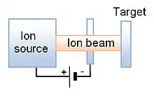 Irradiation at ion accelerator |
| Single ion irradiations are used to fabricate individual micro- and nanostructures such as cones, channels, pins and wires.[20] The technique requires a weak ion beam which can be switched off after one ion has penetrated the target foil. |
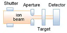 Single ion system |
| Ion microbeams offer the highest level of control of the irradiation process. These restrict the output of a heavy ion accelerator to a small filament which can be scanned over the sample surface. Scribing with individual swift heavy ions is possible with an aiming precision of about one micrometer.[21] |
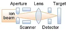 Ion microbeam system |
Formation of ion tracks
When a swift heavy ion penetrates through a solid, it leaves behind a trace of irregular and modified material confined to a cylinder of few nanometers in diameter. The energy transfer between the heavy projectile ion and the light target electrons occurs in binary collisions. The knocked-off primary electrons leave a charged region behind, inducing a secondary electron collision cascade involving an increasing number of electrons of decreasing energy. This electron collision cascade stops when ionization is no longer possible. The remaining energy leads to atomic excitation and vibration, producing (heat). Due to the large proton-to-electron mass ratio, the energy of the projectile decreases gradually and the projectile path is straight.[29] A small fraction of the transferred energy remains as an ion track in the solid. The diameter of the ion track increases with increasing radiation sensitivity of the material. Several models are used to describe ion track formation.
- According to the ion explosion spike model[30] the primary ionization induces an atomic collision cascade,[31] resulting in a disordered zone around the ion trajectory.
- According to the electron collision cascade model the secondary electrons induce a radiation effect in the material, similar to a spatially-confined electron irradiation.[32] The electron collision cascade model is particularly suited for polymers.
- According to the thermal spike model, the electron collision cascade is responsible for the energy transfer between the projectile ion and the target nuclei. If the temperature exceeds the melting temperature of the target substance, a liquid is formed. The rapid quenching leaves behind an amorphous state with decreased density. Its disorder corresponds to the ion track.[3][33]
The thermal spike model suggests the radiation sensitivity of different materials depends on their thermal conductivity and their melting temperature.
 Thermal spike model
Ion track corresponds to frozen disorder after rapid quenching of melt zone around ion trajectory. Temperature represented by color. Ion path vertical to image plane.
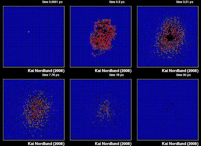 Molecular dynamics simulation of collision cascade in gold.
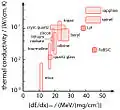 Track etch threshold: energy input required for selective etching. For ionic crystals, the threshold increases with the heat conductivity. Amorphous metal FeBSiC included for comparison.
Etching methods
Selective ion etching
Selective ion track etching[2] is closely related to the selective etching of grain boundaries and crystal dislocations. The etch process must be sufficiently slow to discriminate between the irradiated and the pristine material. The resulting shape depends on the type of material, the concentration of the etchant, and the temperature of the etch bath. In crystals and glasses, selective etching is due to the reduced density of the ion track. In polymers, selective etching is due to polymer fragmentation in the ion track core. The core zone is surrounded by a track halo in which cross-linking can impede track etching. After removal of the cross-linked track halo, the track radius grows linear in time. The result of selective etching is a trough, pore, or channel.
Surfactant enhanced etching
Surfactant enhanced etching is used to modify ion track shapes.[34] It is based on self-organized monolayers.[11] The monolayers are semi-permeable for the solvated ions of the etch medium and reduce surface attack. Depending on the relative concentration of the surfactant and the etch medium, barrel or cylindrical shaped ion track pores are obtained. The technique can be used to increase the aspect ratio.[35]
Other related terminology
Repeated irradiation and processing: A two-step irradiation and etching process used to create perforated wells.
Arbitrary irradiation angles enforce an anisotropy along one specific symmetry axis.
Multiangular channels are interpenetrating networks consisting of two or more channel arrays in different directions.
 Double sided etching of ion track at track etch ratio 5:1.
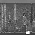 Asymmetric ion track channels with strongly reduced top diameter.
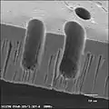 Microwells with perforated bottom.
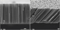 Two membranes with different channel inclination (vertical and 45 degrees).
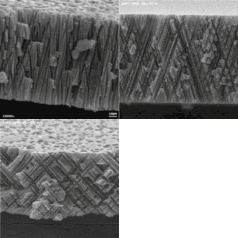 Three membranes perforated at two strutting angles (±10, ±20, ±45 degrees).
| Material | pH | Wet etchant | Sensitizer1) | Desensitizer2) | T/°C3) | Speed4) | Selectivity5) |
|---|---|---|---|---|---|---|---|
| PC | basic | NaOH | UV | Alcohols | 50-80 | Fast | 100-10000 |
| PET | basic | NaOH | UV, DMF | Alcohols | 50-90 | Fast | 10-1000 |
| basic | K2CO3 | 80 | Slow | 1000 | |||
| PI | basic | NaOCl | NaOH | 50-80 | Fast | 100-1000 | |
| CR39 | basic | NaOH | UV | 50-80 | Fast | 10-1000 | |
| PVDF6) | basic | KMnO4 + NaOH | 80 | Medium | 10-100 | ||
| PMMA6) | acidic | KMnO4 + H2SO4 | 50-80 | Medium | 10 | ||
| PP6) | acidic | CrO3 + H2SO4 | 80 | Fast | 10-100 |
1) Sensitizers increase the track etch ratio by breaking bonds or by increasing the free volume.
2) Desensitizers decrease the track etch ratio. Alternatively ion tracks can be thermally annealed.
3) Typical etch bath temperature range. Etch rates increase strongly with concentration and temperature.
4) Axial etching depends on track etch speed vt, radial etching depends on general etch speed vg.
5) Selectivity (aspect ratio, track etch ratio) = track etch speed / general etch speed = vt / vg.
6) This method requires to remove remaining metal oxide deposits by aqueous HCl solutions.
Replication
Etched ion tracks can be replicated by polymers[37] or metals.[12] [38] Replica and template can be used as composite. A replica can be separated from its template mechanically or chemically. Polymer replicas are obtained by filling the etched track with a liquid precursor of the polymer and curing it. Curing can be activated by a catalyst, by ultraviolet radiation, or by heat. Metal replicas can be obtained either by electroless deposition or by electro-deposition. For replication of through-pores, a cathode film is deposited on one side of the membrane, and the membrane is immersed in a metal salt solution. The cathode film is negatively charged with respect to the anode, which is placed on the opposite side of the membrane. The positive metal ions are pulled toward the cathode, where they catch electrons and precipitate as a compact metal film. During electro-deposition, the channels fill gradually with metal, and the lengths of the nano-wires are controlled by the deposition time. Rapid deposition leads to polycrystalline wires, while slow deposition leads to single crystalline wires. A free-standing replica is obtained by removing the template after deposition of a bearing film on the anode side of the membrane.
Interpenetrating wire networks are fabricated by electro-deposition in multi-angle, track-etched membranes. Free-standing three-dimensional networks with tunable complexity and interwire connectivity are obtained.[39]
Segmented nanowires are fabricated by alternating the polarity during electro-deposition.[40] The segment length is adjusted by the pulse duration. In this way electrical, thermal, and optical properties can be tuned.
 Free standing metal replica of etched ion tracks in PC
 Interpenetrating wire network
 Bundle of segmented platinum nanowires
Applications
Microtechnology: The common mechanical tools of the macroworld are being supplemented and complemented, and in some applications replaced by, particle beams. Here, beams of photons and electrons modify the solubility of radiation-sensitive polymers, so-called "resists", while masking protects a selected area from exposure to radiation, chemical attack, and erosion by atomic impact. Typical products produced in this way are integrated circuits and microsystems. At present, the field of microtechnology is expanding toward nanotechnology. A recent branch of microfabrication is based on manipulation of individual ions.
Geology: Ion tracks are useful as they can remain unaltered for millions of years In minerals. Their density yields information about the time when the mineral solidified from its melt, and are used as geological clocks in fission track dating
Filters: Homoporous filters were among the first applications[8] of ion track technology, and are now fabricated by several companies.[41] Mica membranes with ion track pores were used by Beck and Schultz to determine the mechanism of hindered diffusion in nanopores.[42][43]
Classifying micro- and nanoparticles: The resistance of a channel filled by an electrolyte depends on the volume of the particle passing through it.[10] This technique is applied to the counting and sizing of individual red blood cells, bacteria, and virus particles.
pH Sensor: Charged channels filled with an electrolyte have a surface conductivity, in addition to the regular volume conductivity, of the electrolyte. Ions attached to a charged surface attract a cloud of mobile counterions. Fixed and mobile ions form a double layer. For small channels, surface conductivity is responsible for most of the charge transport. For small channels, surface conductivity exceeds volume conductivity. Negative surface charges can be occupied by firmly bound protons. At low pH (high proton concentration), the wall charge is completely neutralized. Surface conductivity vanishes. Due to the dependence of surface conductivity on pH, the channel becomes a pH sensor.[44]
Current rectifying pores: Asymmetric pores are obtained by one-sided etching. The geometric asymmetry translates into a conduction asymmetry. The phenomenon is similar to an electrical valve. The pore has two characteristic conduction states, open and closed. Above a certain voltage the valve opens. Below a certain voltage the valve closes.[45][46]
Thermo-responsive channel: Obtained by lining a channel with a thermo-responsive gel.[47]
Bio-sensor: Chemical modification of the channel wall changes its interaction with passing particles. Different wall claddings bind to specific molecules and delay their passage. In this sense, the wall recognizes the passing particle. As an example, DNA fragments are selectively bound by their complementary fragments. The attached molecules reduce the channel volume. The induced resistance change reflects the molecule's concentration.[48]
Anisotropic conduction: A platform covered with many free standing wires acts as large area field emitter.[49]
Magnetic multilayers: Nano-wires consisting of alternating magnetic/nonmagnetic layers act as magnetic sensors. As an example, cobalt/copper nanowires are obtained from an electrolyte containing both metals. At low voltage, pure copper is deposited while cobalt resists electro-deposition. At high voltage, both metals are deposited as an alloy. If the electrolyte contains predominantly cobalt, a magnetic cobalt-copper alloy is deposited with a high fraction of cobalt. The electrical conductivity of the multilayer wire depends on the applied external magnetic field. The magnetic order of the cobalt layers increases with the applied field. Without magnetic field, neighboring magnetic layers prefer the anti-parallel order. With magnetic field, the magnetic layers prefer the orientation parallel with the magnetic field. The parallel orientation corresponds to a reduced electrical resistance. The effect is used in reading heads of magnetic storage media (the "GMR effect").[50]
Spintronics: Spin valve structure consists of two magnetic layers of different thicknesses. The thick layer has a higher magnetic stability and is used as polarizer. The thin layer acts as analyzer. Depending on its magnetization direction with respect to the polarizer (parallel or antiparallel), its conductivity is low or high, respectively.[51]
Textures: Tilted textures with a hydrophobic coating are at the same time superhydrophobic and anisotropic,[18] and show a preferred direction of transport. The effect has been demonstrated to convert vibration into translation.[52]
 Etched ion tracks
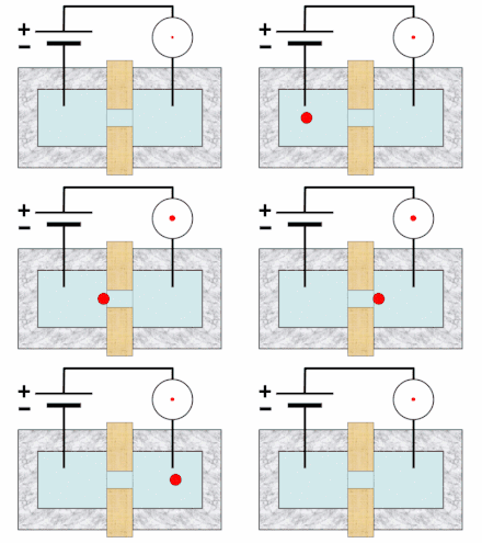 Particle Transit Channel. The transient current drop is proportional to the particle volume.
 pH Sensor: The moving circle represents the cross section of a negatively charged channel. Left: At low pH all surface charges are occupied by protons (low conductivity). Right: At high pH all surface charges are available (high conductivity).
 Asymmetric pore transmits positive ions preferentially from right to left.
 Thermo-responsive channel. The hydrogel-lined channel opens above and closes below the critical temperature of the hydrogel.
 Biospecific Sensor. The electrical resistance of a channel clad with an immuno reactant depends on the concentration of a specific molecule.
 Field emitter array
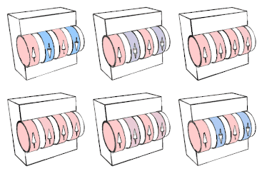 Multilayer Magnetosensor.
Low magnetic field: antiparallel orientation and high resistance.
High magnetic field: parallel orientation and low resistance. Spin Analyzer
The energy loss of spin-polarized electrons depends on the magnetic orientation of the analyzer. Left: polarizer (blue: spin-up). Right: analyzer (blue: spin-up; red: spin-down). Tilted Track Texture with asymmetric transport properties.
Notes
- D.A. Young (1958). "Etching of radiation damage in lithium fluoride". Nature. 182 (4632): 375–377. Bibcode:1958Natur.182..375Y. doi:10.1038/182375a0. PMID 13577844. S2CID 4282512.
-
R.L. Fleischer; P.B. Price; R.M. Walker (1975). Nuclear tracks in solids. pp. 30–9. doi:10.1038/scientificamerican0669-30. ISBN 978-0-520-02665-0. PMID 5769561.
{{cite book}}:|journal=ignored (help) -
F. Seitz; J.S. Koehler (1956). F. Seitz; D. Turnbull (eds.). "Solid State Physics". Academic Press: 307. LCCN 55012299.
{{cite journal}}: Cite journal requires|journal=(help) - M. Toulemonde; C. Dufour; A. Meftah; E. Paumier (2000). "Transient thermal processes in heavy ion irradiation of crystalline inorganic insulators". Nuclear Instruments and Methods B. 166–167: 903–912. Bibcode:2000NIMPB.166..903T. doi:10.1016/S0168-583X(99)00799-5.
- G. Remmert; Y. Eyal; B.E. Fischer; R. Spohr (1995). "Gas permeability and cross section of latent ion tracks in polymers". Nuclear Instruments and Methods B. 105 (1–4): 197–199. Bibcode:1995NIMPB.105..197R. doi:10.1016/0168-583X(95)00576-5.
- R. Spohr (1990). Ion tracks and microtechnology. Vieweg Verlag. ISBN 978-3-528-06330-6.
- W. D. Williams; N. Giordano (1984). "Fabrication of 80 Å metal wires". Review of Scientific Instruments. 55 (3): 410–412. Bibcode:1984RScI...55..410W. doi:10.1063/1.1137752.
- R.L. Fleischer; P.B. Price; R.M. Walker (1963). "Method of forming fine holes of near atomic dimensions". Review of Scientific Instruments. 34 (5): 510–512. Bibcode:1963RScI...34..510F. doi:10.1063/1.1718419.
- P. Apel (2003). "Swift ion effects in polymers: industrial applications". Nuclear Instruments and Methods in Physics Research Section B. 208: 11–20. Bibcode:2003NIMPB.208...11A. doi:10.1016/S0168-583X(03)00634-7.
- R.W. DeBlois; C.P. Bean (1970). "Counting and sizing of submicron particles by the resistive pulse technique". Review of Scientific Instruments. 41 (7): 909–916. Bibcode:1970RScI...41..909D. doi:10.1063/1.1684724.
- W.J. Petzny; J.A. Quinn (1969). "Calibrated membranes with coated pore walls". Science. 166 (3906): 751–753. Bibcode:1969Sci...166..751P. doi:10.1126/science.166.3906.751. PMID 5823313. S2CID 1807195.
- G.E. Possin (1970). "A method for forming very small diameter wires". Review of Scientific Instruments. 41 (5): 772–774. Bibcode:1970RScI...41..772P. doi:10.1063/1.1684640.
- J. Vetter. "Free standing metal whiskers". GSI Darmstadt. Retrieved 2010-04-27.
- Y. Eyal; K. Gassan (1999). "Observation of latent heavy-ion tracks in polyimide by means of transmission electron microscopy". Nuclear Instruments and Methods in Physics Research B. 156 (1–4): 183–190. Bibcode:1999NIMPB.156..183E. doi:10.1016/S0168-583X(99)00269-4.
- J.F. Ziegler (1980). Handbook of Stopping Cross-Sections for Energetic Ions in All Elements. Pergamon Press. ISBN 978-0080216072.
- "Stopping and Range Calculation". Srim.org. Retrieved 2013-01-21.
- M. Lindeberg; K. Hjort (2004). "A comprehensive study of ion track enabled high aspect ratio microstructures in flexible circuit boards". Microsystem Technologies. 10 (8–9): 608–621. doi:10.1007/s00542-003-0339-2. S2CID 109327888.
- R. Spohr; G. Sharma; P. Forsberg; M. Karlsson; A. Hallén; L. Westerberg (2010). "Stroke Asymmetry of Tilted Superhydrophobic Ion Track Textures". Langmuir. 26 (9): 6790–6796. doi:10.1021/la904137t. PMID 20085343.
- C. Riedel; R. Spohr (1980). "Transmission Properties of Nuclear Track Filters". Journal of Membrane Science. 7 (2): 225–234. doi:10.1016/S0376-7388(00)80083-6.
- R. Spohr; C. Zet; B.E. Fischer; H. Kiesewetter; P. Apel; I. Gunko; L. Westerberg (2010). "Controlled fabrication of ion track nanowires and channels". Nuclear Instruments and Methods in Physics Research B. 268 (6): 676–686. Bibcode:2010NIMPB.268..676S. doi:10.1016/j.nimb.2009.12.017. hdl:10069/32233.
- B.E. Fischer; M. Heiss; M. Cholewa (2003). "About the art to shoot with single ions". Nuclear Instruments and Methods in Physics Research B. 210: 285–291. Bibcode:2003NIMPB.210..285F. doi:10.1016/S0168-583X(03)01038-3.
- "Table of Nuclides". Atom.kaeri.re.kr. Retrieved 2013-01-21.
- "Interactive Chart of Nuclides". Nndc.bnl.gov. Retrieved 2013-01-21.
- 102 fission events/s
- Brookhaven Tandem Van de Graaf
- GSI Irradiation Facilities Archived March 13, 2008, at the Wayback Machine
- "High Volage Accelerator Systems". Highvolteng.com. Retrieved 2013-01-21.
- "Estimate Coulomb barrier". Physicsconsult.de. Retrieved 2013-01-21.
- For iron, the mass ratio MFe/me~ 105
- R. L. Fleischer; P.B. Price; R.M. Walker (1965). "Ion Explosion Spike Mechanism for Formation of Charged‐Particle Tracks In Solids". Journal of Applied Physics. 36 (11): 3645–3652. Bibcode:1965JAP....36.3645F. doi:10.1063/1.1703059.)
-
K. Nordlund, M. Ghaly, R. S. Averback, M. Caturla, T. Diaz de la Rubia, J. Tarus (1998). "Defect production in collision cascades in elemental semiconductors and FCC metals". Physical Review B. 57 (13): 7556. Bibcode:1998PhRvB..57.7556N. doi:10.1103/PhysRevB.57.7556.
{{cite journal}}: CS1 maint: multiple names: authors list (link)) - R. Katz (1978). "Track Structure Theory In Radiobiology and In Radiation Detection". Nuclear Track Detection. 2 (1): 1–28. doi:10.1016/0145-224X(78)90002-9.
- M. Toulemonde; C. Dufour; A. Meftah; E. Paumier (2000). "Transient thermal processes In heavy ion irradiation of crystalline inorganic insulators". Nuclear Instruments and Methods B. 166–167: 903–912. Bibcode:2000NIMPB.166..903T. doi:10.1016/S0168-583X(99)00799-5.
-
P.Y.Apel, I.V. Blonskaya, A.Y. Didyk, S.N. Dmitriev, O.L. Orelovitch, D. Root, L.I. Samoilova, V.A. Vutsadakis (2001). "Surfactant-enhanced control of track-etch pore morphology". Nuclear Instruments and Methods in Physics Research Section B. 179 (1): 55–62. Bibcode:2001NIMPB.179...55A. doi:10.1016/S0168-583X(00)00691-1.
{{cite journal}}: CS1 maint: multiple names: authors list (link) - L.C.T. Man; P. Apel; T. Cheung; L. Westerberg; K.N. Yu; C. Zet; R. Spohr (2007). "Influence of a surfactant on single ion track etching. Preparing and manipulating individual cylindrical micro wires". Nuclear Instruments and Methods in Physics Research Section B. 265 (2): 621–625. Bibcode:2007NIMPB.265..621M. doi:10.1016/j.nimb.2007.09.029.
- "P. Apel, R. Spohr: Introduction to ion track etching in polymers". Ion-tracks.de. Retrieved 2013-01-21.
- P.B. Price; G.M. Comstock; R.L. Fleischer; W.R. Giard; H.R. Hart; G.E. Nichols (1971). "Cosmic-Ray Tracks in Plastics: The Apollo Helmet Dosimetry Experiment". Science. 172 (3979): 154–157. Bibcode:1971Sci...172..154C. doi:10.1126/science.172.3979.154. PMID 17735223. S2CID 13108585.
- See: plating and electroplating
- M. Rauber; I. Alber; S. Müller; R. Neumann; O. Picht; C. Roth; A. Schöckel; M.E. Toimil-Molares; W. Ensinger (2011). "Highly-Ordered Supportless Three-Dimensional Nanowire Networks with Tunable Complexity and Interwire Connectivity for Device Integration". Nano Letters. 11 (6): 2304–2310. Bibcode:2011NanoL..11.2304R. doi:10.1021/nl2005516. PMID 21608990.
- M. Rauber; J. Brötz; J. Duan; J. Liu; S. Müller; R. Neumann; O. Picht; M.E. Toimil-Molares; W. Ensinger (2010). "Segmented All-Platinum Nanowires with Controlled Morphology through Manipulation of the Local Electrolyte Distribution in Fluidic Nanochannels during Electrodeposition". Journal of Physical Chemistry C. 114 (51): 22502–22507. doi:10.1021/jp108889c.
- "Ion track companies". Physicsconsult.de. 2011-07-04. Retrieved 2013-01-21.
- Beck, R. E.; Schultz, J. S. (1970-12-18). "Hindered Diffusion in Microporous Membranes with Known Pore Geometry". Science. 170 (3964): 1302–1305. Bibcode:1970Sci...170.1302B. doi:10.1126/science.170.3964.1302. ISSN 0036-8075. PMID 17829429. S2CID 43124555.
- Beck, Robert E.; Schultz, Jerome S. (January 1972). "Hindrance of solute diffusion within membranes as measured with microporous membranes of known pore geometry". Biochimica et Biophysica Acta (BBA) - Biomembranes. 255 (1): 273–303. doi:10.1016/0005-2736(72)90028-4. hdl:2027.42/34175. PMID 4334681.
- A. Wolf; N. Reber; P. Yu. Apel; B.E. Fischer; R. Spohr (1995). "Electrolyte transport in charged single ion track capillaries". Nuclear Instruments and Methods in Physics Research B. 105 (1–4): 291–293. Bibcode:1995NIMPB.105..291W. doi:10.1016/0168-583X(95)00577-3.
-
P.Y. Apel, Y.E. Korchev, Z. Siwy, Z.; R. Spohr, M. Yoshida (2001). "Diode-like single-ion track membrane prepared by electro-stopping". Nuclear Instruments and Methods in Physics Research B. 184 (3): 337–346. Bibcode:2001NIMPB.184..337A. doi:10.1016/S0168-583X(01)00722-4.
{{cite journal}}: CS1 maint: multiple names: authors list (link) - P. Ramirez; P.Yu. Apel; J. Cervera; S. Mafe (2008). "Pore structure and function of synthetic nanopores with fixed charges: tip shape and rectification properties". Nanotechnology. 19 (31): 315707. Bibcode:2008Nanot..19E5707R. doi:10.1088/0957-4484/19/31/315707. PMID 21828799. S2CID 43193256.
- M. Tamada; M. Yoshida; M. Asano; H. Omichi; R. Katakai; R. Spohr; J. Vetter (1992). "Thermo-response of ion track pores in copolymer films of methacryloyl-L-alaninemethylester and diethyleneglycol-bis-allylcarbonate (CR-39)". Polymer. 33 (15): 3169–3172. doi:10.1016/0032-3861(92)90230-T.
- L.T. Sexton; L.P. Horne; C.R. Martin (2007). "Developing synthetic conical nanopores for biosensing applications". Molecular BioSystems. 3 (10): 667–685. doi:10.1039/b708725j. PMID 17882330.
- F. Maurer; A. Dangwal; D. Lysenkov; G. Müller; M.E. Toimil-Molares; C. Trautmann; J. Brötz; H. Fuess (2006). "Field emission of copper nanowires grown in polymer ion-track membranes". Nuclear Instruments and Methods in Physics Research B. 245 (1): 337–341. Bibcode:2006NIMPB.245..337M. doi:10.1016/j.nimb.2005.11.124.
- L. Piraux; J.M. George; J.F. Despres; C. Leroy; E. Ferain; R. Legras; K. Ounadjela; A. Fert (1994). "Giant magnetoresistance in magnetic multilayered nanowires". Applied Physics Letters. 65 (19): 2484–2486. Bibcode:1994ApPhL..65.2484P. doi:10.1063/1.112672.
- B. Doudin; J.P. Ansermet (1997). "Nanostructuring materials for spin electronics". Europhysics News. 28 (1): 14–17. Bibcode:1997ENews..28...14D. doi:10.1007/s00770-997-0014-8. S2CID 123078833.
- "Converting vibration into translation". Retrieved 2013-01-21.
External links
 Media related to Ion track at Wikimedia Commons