Pentium
Pentium is a discontinued series of x86 architecture-compatible microprocessors produced by Intel. The original Pentium was first released on March 22, 1993.
 First Pentium logo (1993) | |
| General information | |
|---|---|
| Launched | March 22, 1993 |
| Discontinued | 2023[1] |
| Common manufacturer(s) | |
| Performance | |
| Max. CPU clock rate | 50 MHz to 4.4 GHz |
| FSB speeds | 50 MHz to 800 MT/s |
| DMI speeds | 2 GT/s to 16 GT/s |
| Architecture and classification | |
| Technology node | 800 nm to Intel 7 |
| Microarchitecture | |
| Instruction set | IA-32, x86-64 |
| Instructions | x86 |
| Physical specifications | |
| Cores |
|
| Socket(s) | |
| Products, models, variants | |
| Brand name(s) |
|
| Variant(s) | |
| History | |
| Predecessor(s) | i486 |
| Successor(s) | Core |
Pentium-branded processors released from 2009 to 2022 are considered entry-level products that Intel rates as "two stars",[2][3] meaning that they are above the low-end Atom and Celeron series, but below the faster Intel Core lineup and workstation/server Xeon series. These later Pentium processors have little more than their name in common with earlier Pentiums, which were Intel's flagship processor for over a decade until the introduction of the Intel Core line in 2006. They are based on both the architecture used in Atom and that of Core processors. In the case of Atom architectures, Pentiums are the highest performance implementations of the architecture. Pentium processors with Core architectures prior to 2017 were distinguished from the faster, higher-end i-series processors by lower clock rates and disabling some features, such as hyper-threading, virtualization and sometimes L3 cache.
The name "Pentium" is originally derived from the Greek word pente (πεντε), meaning "five", a reference to the prior numeric naming convention of Intel's 80x86 processors (8086–80486), with the Latin ending -ium since the processor would otherwise have been named 80586 using that convention.
In 2017, Intel split Pentium into two line-ups:
- Pentium Silver, aiming for low-power devices and shares architecture with Atom and Celeron.
- Pentium Gold, aiming for entry-level desktop and using existing architecture, such as Kaby Lake or Coffee Lake.
In September 2022, Intel announced that the Pentium and Celeron brands will be replaced with the new "Intel Processor" branding for low-end processors in desktops and laptops from 2023 onwards.[1]
Overview
During development, Intel generally identifies processors with codenames, such as Prescott, Willamette, Coppermine, Katmai, Klamath, or Deschutes. These usually become widely known,[4] even after the processors are given official names on launch.
| Brand | Microarchitecture | Desktop | Laptop | Server |
|---|---|---|---|---|
| Pentium Pentium OverDrive |
P5 | P5 (0.8 μm) P54C (0.6 μm) P54CS (0.35 μm) | ||
| Pentium MMX Pentium OverDrive MMX |
P55C (0.35 μm) Tillamook (0.25 μm) | |||
| Pentium Pro | P6 | P6 (0.5 μm) P6 (0.35 μm) | ||
| Pentium II Pentium II Xeon Pentium II OverDrive Mobile Pentium II |
Klamath (0.35 μm) Deschutes (0.25 μm) | Tonga (0.25 μm) Dixon (0.25 μm) Dixon (0.18 μm) | Drake (0.25 μm) | |
| Pentium III Pentium III Xeon Mobile Pentium III Pentium III M |
Katmai (0.25 μm) Coppermine (180 nm) Tualatin (130 nm) | Coppermine (180 nm) Tualatin(130 nm) | Tanner (0.25 μm) Cascades (180 nm) | |
| Pentium 4 Pentium 4 Extreme Edition |
NetBurst | Willamette (180 nm) Northwood (130 nm) Gallatin (130 nm) Prescott-2M (90 nm) Prescott (90 nm) Cedar Mill (65 nm) | Northwood (130 nm) Prescott (90 nm) | Rebranded as Xeon |
| Pentium D Pentium Extreme Edition |
Smithfield (90 nm) Presler (65 nm) | |||
| Pentium M | P6 based | Banias (130 nm) Dothan (90 nm) | ||
| Pentium Dual-Core | Yonah (65 nm) | |||
| Core | Allendale (65 nm) Wolfdale-3M (45 nm) | Merom-2M (65 nm) | ||
| Pentium | Core | Wolfdale-3M (45 nm) | Penryn-3M (45 nm) | |
| Nehalem | Clarkdale (32 nm) | Arrandale (32 nm) | ||
| Sandy Bridge | Sandy Bridge (32 nm) | |||
| Ivy Bridge | Ivy Bridge (22 nm) | |||
| Haswell | Haswell (22 nm) | |||
| Broadwell | Broadwell (14 nm) | |||
| Skylake | Skylake (14 nm) | Braswell; Goldmont | ||
| Kaby Lake | Kaby Lake (14 nm) | Goldmont Plus (Gemini Lake) | ||
| Coffee Lake | Coffee Lake (14 nm) | |||
| Comet Lake | Comet Lake (14 nm) | |||
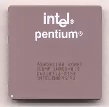
The original Pentium-branded CPUs were expected to be named 586 or i586, to follow the naming convention of prior generations (286, i386, i486). However, as the firm wanted to prevent their competitors from branding their processors with similar names (as AMD had done with their Am486), Intel filed a trademark application on the name in the United States, but was denied because a series of numbers was considered to lack trademark distinctiveness.[5]
Following Intel's prior series of 8086, 80186, 80286, 80386, and 80486 microprocessors, the firm's first P5-based processor was released as the original Intel Pentium on March 22, 1993. Marketing firm Lexicon Branding was hired to coin a name for the new processor. The suffix -ium was chosen as it could connote a fundamental ingredient of a computer, like a chemical element,[6] while the prefix pent- could refer to the fifth generation of x86.[5]
Due to its success, the Pentium brand would continue through several generations of high-end processors. In 2006, the name briefly disappeared from Intel's technology roadmaps,[7][8] only to re-emerge in 2007.[9]
In 1998, Intel introduced the Celeron[10] brand for low-priced processors. With the 2006 introduction of the Intel Core brand as the company's new flagship line of processors, the Pentium series was to be discontinued. However, due to a demand for mid-range dual-core processors, the Pentium brand was repurposed to be Intel's mid-range processor series, between the Celeron and Core series, continuing with the Pentium Dual-Core line.[11][12][13]
In 2009, the "Dual-Core" suffix was dropped, and new x86 processors started carrying the plain Pentium name again.
In 2014, Intel released the Pentium 20th Anniversary Edition, to mark the 20th anniversary of the Pentium brand. These processors are unlocked and highly overclockable.
In 2017, Intel split the Pentium branding into two line-ups. Pentium Silver targets low-power devices and shares architecture with Atom and Celeron, while Pentium Gold targets entry-level desktops and uses existing architecture, such as Kaby Lake and Coffee Lake.
In September 2022, Intel announced that the Pentium and Celeron brands will be replaced with the new "Intel Processor" branding for low-end processors in laptops from 2023 onwards.[1]
Pentium-branded processors
P5 microarchitecture based
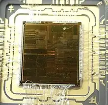
The original Intel P5 or Pentium and Pentium MMX processors were the superscalar follow-on to the 80486 processor and were marketed from 1993 to 1999. Some versions of these were available as Pentium OverDrive that would fit into older CPU sockets.
Pentium
| Core p | Process | Clock rates | L1 cache | FSB | Socket | Release date |
|---|---|---|---|---|---|---|
| P5 | 0.8 μm | 60–66 MHz | 16 KB | 60–66 MHz | Socket 4 | March 1993 |
| P54C | 0.6 μm | 75–120 MHz | 16 KB | 50–66 MHz | Socket 5 | October 1994 |
| P54CS | 0.35 μm | 133–200 MHz | 16 KB | 60–66 MHz | Socket 7 | June 1995 |
| P55C | 0.35 μm | 120–233 MHz | 32 KB | 60–66 MHz | Socket 7 | January 1997[14] |
| Tillamook | 0.25 μm | 166–300 MHz | 32 KB | 66 MHz | Socket 7 | August 1997 |
P6 microarchitecture based
In parallel with the P5 microarchitecture, Intel developed the P6 microarchitecture and started marketing it as the Pentium Pro for the high-end market in 1995. It introduced out-of-order execution and an integrated second-level cache on dual-chip processor package. The second P6 generation replaced the original P5 with the Pentium II and rebranded the high-end version as Pentium II Xeon. It was followed by a third version named the Pentium III and Pentium III Xeon respectively. The Pentium II line added the MMX instructions that were also present in the Pentium MMX.
Versions of these processors for the laptop market were initially named Mobile Pentium II and Mobile Pentium III, later versions were named Pentium III-M. Starting with the Pentium II, the Celeron brand was used for low-end versions of most Pentium processors with a reduced feature set such as a smaller cache or missing power management features.
Pentium Pro
| Core | Process | Clock rates | L2 cache | FSB | Socket | Release date |
|---|---|---|---|---|---|---|
| P6 | 0.5 μm | 150 MHz | 256 KB | 60–66 MHz | Socket 8 | November 1995 |
| P6 | 0.35 μm | 166–200 MHz | 256–1024 KB | 60–66 MHz | Socket 8 |
Pentium II
| Core | Process | Clock rates | L2 cache | FSB | Socket | Release date |
|---|---|---|---|---|---|---|
| Klamath | 0.35 μm | 233–300 MHz | 512 KB | 66 MHz | Slot 1 | May 1997 |
| Deschutes | 0.25 μm | 266–450 MHz | 512 KB | 66–100 MHz | Slot 1 | January 1998 |
| Tonga | 0.25 μm | 233–300 MHz | 512 KB | 66 MHz | MMC-2 | April 1998 |
| Dixon | 0.25 μm | 266–366 MHz | 256 KB | 66 MHz | MMC-2 | January 1999 |
Pentium III
| Core | Process | Clock rates | L2 cache | FSB | Socket | Release date |
|---|---|---|---|---|---|---|
| Katmai | 0.25 μm | 450–600 MHz | 512 KB | 100–133 MHz | Slot 1 | February 1999 |
| Coppermine | 0.18 μm | 400 MHz–1.13 GHz | 256 KB | 100–133 MHz | Slot 1, Socket 370, BGA2, μPGA2 | October 1999 |
| Tualatin | 0.13 μm | 700 MHz–1.4 GHz | 512 KB | 100–133 MHz | Socket 370, BGA2, μPGA2 | July 2001 |
NetBurst microarchitecture based
In 2000, Intel introduced a new microarchitecture named NetBurst, with a much longer pipeline enabling higher clock frequencies than the P6-based processors. Initially, these were named Pentium 4, and the high-end versions have since been named simply Xeon. As with Pentium III, there are both Mobile Pentium 4 and Pentium 4 M processors for the laptop market, with Pentium 4 M denoting the more power-efficient versions. Enthusiast versions of the Pentium 4 with the highest clock rates were named Pentium 4 Extreme Edition.
The Pentium D was the first multi-core Pentium, integrating two Pentium 4 chips in one package and was available as the enthusiast Pentium Extreme Edition.
Pentium 4
| Core | Process | Clock rates | L2 cache | FSB rates | Socket | Release date |
|---|---|---|---|---|---|---|
| Willamette | 180 nm | 1.3–2.0 GHz | 256 KB | 400 MT/s | Socket 423, Socket 478 | November 2000 |
| Northwood | 130 nm | 1.6–3.4 GHz | 512 KB | 400 MT/s–800 MT/s | Socket 478 | January 2002 |
| Gallatin | 130 nm | 3.2–3.46 GHz | 512 KB + 2 MB L3 | 800–1066 MT/s | Socket 478, LGA 775 | November 2003 |
| Prescott | 90 nm | 2.4–3.8 GHz | 1 MB | 533 MT/s–800 MT/s | Socket 478, LGA 775 | February 2004 |
| Prescott-2M | 90 nm | 2.8–3.8 GHz | 2 MB | 800–1066 MT/s | LGA 775 | February 2005 |
| Cedar Mill | 65 nm | 3.0–3.6 GHz | 2 MB | 800 MT/s | LGA 775 | January 2006 |
Pentium D
| Core | Process | Clock rates | L2 cache | FSB rates | Socket | Release date |
|---|---|---|---|---|---|---|
| Smithfield | 90 nm | 2.66–3.2 GHz | 2 MB | 533–800 MT/s | LGA 775 | May 2005 |
| Smithfield XE | 90 nm | 3.2 GHz | 2 MB | 800 MT/s | LGA 775 | May 2005 |
| Presler | 65 nm | 2.8–3.6 GHz | 4 MB | 800 MT/s | LGA 775 | January 2006 |
| Presler XE | 65 nm | 3.46–3.73 GHz | 4 MB | 1066 MT/s | LGA 775 | January 2006 |
Pentium M microarchitecture based
In 2003, Intel introduced a new processor based on the P6 microarchitecture named Pentium M, which was much more power-efficient than the Mobile Pentium 4, Pentium 4 M, and Pentium III M. Dual-core versions of the Pentium M were developed under the code name Yonah and sold under the marketing names Core Duo and Pentium Dual-Core. Unlike Pentium D, it integrated both cores on one chip. From this point, the Intel Core brand name was used for the mainstream Intel processors, and the Pentium brand became a low-end version between Celeron and Core. All Pentium M based designs including Yonah are for the mobile market.
Pentium M
| Core | Process | Clock rates | L1 cache | L2 cache | FSB | Socket | Release date |
|---|---|---|---|---|---|---|---|
| Banias | 130 nm | 0.9–1.7 GHz | 64 KB | 1 MB | 400 MT/s | Socket 479 | March 2003 |
| Dothan | 90 nm | 1.00–2.26 GHz | 64 KB | 2 MB | 400–533 MT/s | FC-uBGA | June 2004 |
Pentium Dual-Core
| Core | Process | Clock rates | L1 cache | L2 cache | FSB rates | Socket | Release date |
|---|---|---|---|---|---|---|---|
| Yonah | 65 nm | 1.6–1.86 GHz | 64 KB | 1 MB | 533 MT/s | Socket M | January 2007 |
Core microarchitecture based
The Pentium Dual-Core name continued to be used when the Yonah design was extended with 64-bit support, now named the Core microarchitecture. This eventually replaced all NetBurst-based processors across the four brands Celeron, Pentium, Core, and Xeon. Pentium Dual-Core processors based on the Core microarchitecture use the Allendale and Wolfdale-3M designs for desktop processors and Merom-2M for mobile processors.
Pentium Dual-Core
| Core | Process | Clock rates | L1 cache | L2 cache | FSB rates | Socket | Release date |
|---|---|---|---|---|---|---|---|
| Merom-2M | 65 nm | 1.46–2.16 GHz | 64 KB | 1 MB | 533–667 MT/s | Socket P | Q4 2007 |
| Allendale | 65 nm | 1.6–2.4 GHz | 64 KB | 1 MB | 800 MT/s | Socket 775 | June 2007 |
| Wolfdale-3M | 45 nm | 2.2–2.7 GHz | 64 KB | 2 MB | 800 MT/s | Socket 775 | August 2008 |
Pentium (2009)
| Core | Process | Clock rates | L1 cache | L2 cache | FSB rates | Socket | Release date |
|---|---|---|---|---|---|---|---|
| Wolfdale-3M | 45 nm | 2.8–3.2 GHz | 64 KB | 2 MB | 1066 MT/s | Socket 775 | May 2009 |
| Penryn-3M | 45 nm | 2.0–2.3 GHz | 64 KB | 1 MB | 800 MT/s | Socket P | January 2009 |
| Penryn-3M ULV | 45 nm | 1.3–1.5 GHz | 64 KB | 2 MB | 800 MT/s | BGA 956 | September 2009 |
| Penryn-L ULV 1 | 45 nm | 1.3–1.4 GHz | 64 KB | 2 MB | 800 MT/s | BGA 956 | May 2009 |
| Codename | Brand name | Model (list) | Cores | L2 cache | Socket | TDP |
|---|---|---|---|---|---|---|
| Allendale | Pentium Dual-Core | E2xxx | 2 | 1 MB | LGA 775 | 65 W |
| Merom-2M | Mobile Pentium Dual-Core | T2xxx T3xxx | 2 | 1 MB | Socket P | 35 W |
| Wolfdale-3M | Pentium Dual-Core | E2xxx | 2 | 1 MB | LGA 775 | 65 W |
| E5xxx | 2 MB | |||||
| Pentium | E6xxx | |||||
| Penryn-3M | Mobile Pentium | T4xxx | 2 | 1 MB | Socket P | 35 W |
| SU4xxx | 2 MB | μFC-BGA 956 | 10 W | |||
| Penryn-L | SU2xxx | 1 | 5.5 W |
In 2009, Intel changed the naming system for Pentium processors, renaming the Wolfdale-3M based processors to Pentium, without the Dual-Core name, and introduced new single- and dual-core processors based on Penryn under the Pentium name.
The Penryn core is the successor to the Merom core and Intel's 45 nm version of their mobile series of Pentium processors. The FSB frequency is increased from 667 MHz to 800 MHz, and the voltage is lowered. Intel released the first Penryn Core, the Pentium T4200, in December 2008. In June 2009, Intel released the first single-core processor to use the Pentium name, a Consumer Ultra-Low Voltage (CULV) Penryn core named Pentium SU2700.
In September 2009, Intel introduced the Pentium SU4000 series together with the Celeron SU2000 and Core 2 Duo SU7000 series, which are dual-core CULV processors based on Penryn-3M and using 800 MHz FSB. The Pentium SU4000 series has 2 MB L2 cache but is otherwise basically identical to the other two lines.
Nehalem microarchitecture based
The Nehalem microarchitecture was introduced in late 2008 as a successor to the Core microarchitecture, and in early 2010, a new Pentium G6950 processor based on the Clarkdale design was introduced based on the Westmere refresh of Nehalem, which were followed by the mobile P6xxx based on Arrandale a few months later.
| Core | Process | Clock rates | L2 cache | L3 cache | I/O bus | Socket | Release date |
|---|---|---|---|---|---|---|---|
| Clarkdale | 32 nm | 2.8 GHz | 512 KB | 3 MB | DMI | Socket 1156 | January 2010 |
| Arrandale | 32 nm | 1.2–1.86 GHz | 512 KB | 3 MB | DMI | Socket 988 BGA | Q2 2010 |
| Codename | Brand name | L3 cache | Socket | TDP | Features |
|---|---|---|---|---|---|
| Clarkdale | Pentium G6xxx | 3 MB | LGA 1156 | 73 W | Integrated GPU |
| Arrandale | Pentium P6xxx | 3 MB | LGA 1156 | 35 W | Integrated GPU |
| Pentium U5xxx | BGA | 18 W |
On January 7, 2010, Intel launched a new Pentium model using the Clarkdale chip in parallel with other desktop and mobile CPUs based on their new Westmere microarchitecture. The first model in this series is the Pentium G6950. The Clarkdale chip is also used in the Core i3-5xx and Core i5-6xx series and features a 32 nm process (as it is based on the Westmere microarchitecture), integrated memory controller and 45 nm graphics controller and a third-level cache. In the Pentium series, some features of Clarkdale are disabled, including AES-NI, hyper-threading (versus Core i3), and the graphics controller in the Pentium runs at 533 MHz, while in the Core i3 i3-5xx series they run at 733 MHz, and Dual Video Decode that enables Blu-ray picture-in picture hardware acceleration, and support for Deep Color and xvYCC. The memory controller in the Pentium supports DDR3-1066 max, the same as the Core i3 i3-5xx series.[15] The L3 cache is also 1 MB less than in the Core i3-5xx series.
Sandy Bridge microarchitecture based
The Sandy Bridge microarchitecture was released in the Pentium line on May 22, 2011.
- aAll models share the following details: 2 cores, 2 logical processors (4 on Pentium 3xx with hyper-threading), CPUID signature 206A7, family 6 (06h), model 42 (02Ah), stepping 7 (07h)
- bTranslation lookaside buffer (TLB) and cache 64-byte prefetching; data TLB0 2-MB or 4-MB pages, 4-way associative, 32 entries; data TLB 4-KB pages, 4-way set associative, 64 entries; instruction TLB 4-KB pages, 4-way set associative, 128 entries, L2 TLB 1-MB, 4-way set associative, 64-byte line size; shared 2nd-level TLB 4 KB pages, 4-way set associative, 512 entries.
- cAll models feature: on-chip floating-point unit, Enhanced Intel SpeedStep Technology (EIST), Intel 64, XD bit (an NX bit implementation), Intel VT-x, Smart Cache.
- dAll models support: MMX, SSE, SSE2, SSE3, SSSE3, SSE4.1, SSE4.2
- eHD Graphics (Sandy Bridge) contain 6 EUs and HD Graphics 2000, but does not support these technologies: Intel Quick Sync Video, InTru 3D, Clear Video HD, Wireless Display, 3D Video, or 3D graphics acceleration.
| Codename | Brand namea | L3 cacheb | Socket | TDP | Featuresc,d |
|---|---|---|---|---|---|
| Sandy Bridge | Pentium 3xx | 3 MB | LGA 1155 | 15 W | hyper-threading, ECC |
| Pentium 9x7 | 2 MB | BGA1023 | 17 W | Integrated GPU | |
| Pentium B9x0 | 2 MB | rPGA988B | 35 W | Integrated GPU | |
| Pentium G6xxT[16] | 3 MB, 8-way set associative, 64 byte line size | LGA 1155 | 35 W | Integrated GPUe | |
| Pentium G6xx[17] | 65 W | ||||
| Pentium G8xx[18][19] | 3 MB, 12-way set associative, 64 byte line size | ||||
| Sandy Bridge-EN | Pentium 140x | 5 MB | LGA 1356 | 40–80 W | ECC, AVX, TXT, Intel VT-d, AES-NI |
Ivy Bridge microarchitecture based
Currently, there exist Ivy Bridge models G2010, G2020, G2120, G2030, and G2130. All are dual-core and have no hyper-threading or Turbo Boost.
| Codename | Brand name | L3 cache | Socket | TDP | Notes |
|---|---|---|---|---|---|
| Ivy Bridge | G2010, G2020, G2030, G2120,[20] G2130 | 3 MB | LGA 1155 | 55 W | w/o hyper-threading |
Haswell microarchitecture based
Several Haswell-based Pentium processors were released in 2013, among them the G3258 "Anniversary Edition", first released in 2014 by Intel to commemorate the 20th anniversary of the line. As with prior-generation Pentium processors, Haswell and Haswell Refresh-based parts have two cores only, lack support for hyper-threading, and use the LGA1150 socket form factor.
Broadwell microarchitecture based
Broadwell-based Pentiums were launched in Q1 2015 using a 14 nm process (e.g. the dual-core 1.9 GHz Intel Pentium 3805U with 2 MB cache). They used the FCBGA1168 socket.
Skylake microarchitecture based
Skylake-based Pentium processors support up to 64 GB RAM. Features like Turbo Boost, Intel vPro, Hyper-Threading are not available. Supports AES-NI and RDRAND.[21]
Integrated graphics are provided by Intel HD Graphics 510, utilizing a maximum of 1.7 GB of memory, for resolutions up to 4096×2304 @ 60 Hz using Display Port supporting up to 3 displays.[22]
Kaby Lake microarchitecture based
In Q1 2017 Intel released the Kaby Lake-based Pentium G4560; it is the first Pentium-branded CPU since the NetBurst-based Pentium 4 to support hyper-threading, a feature available in some "Core"-branded products. Features include a clock speed of 3.5 GHz with four threads, 3 MB of L3 cache and Intel HD 610 integrated graphics.
Coffee Lake microarchitecture based
All Coffee Lake Pentium processors support Hyper-threading,[23] and integrated Intel UHD Graphics.
Comet Lake microarchitecture based
All Comet Lake Pentium processors support Hyper-threading, and integrated Intel UHD 610 Graphics.
Pentium-compatible Intel processors
Due to its prominence, the term "Pentium-compatible" is often used to describe any x86 processor that supports the IA-32 instruction set and architecture. Even though they do not use the Pentium name, Intel also manufactures other processors based on the Pentium series for other markets. Most of these processors share the core design with one of the Pentium processor lines, usually differing in the amount of CPU cache, power efficiency or other features. The notable exception is the Atom line, which is an independent design.
- Celeron, a low-end version
- Core, the mainstream version including Core 2, Core i3, Core i5, Core i7 and Core i9, now placed above Pentium
- Xeon, a high-end version used in servers and workstations
- A100 (discontinued), an ultra-mobile version of Pentium M, succeeded by Intel Atom
- EP80579, a system-on-a-chip based on Pentium M
- Xeon Phi, a high-end version used in servers and workstations
- Intel Quark, a now-discontinued, low-power reimplementation of the Pentium architecture for use as microcontroller and in other embedded applications
See also
- List of Intel Pentium processors
- Intel Inside
- Pentium FDIV bug, a well-publicized flaw in the original processor
- Performance Rating, informally termed Pentium Rating
- "It's All About the Pentiums", a song by "Weird Al" Yankovic
- Athlon
References
- Warren, Tom (September 16, 2022). "Intel Processor will replace Pentium and Celeron in 2023 laptops". The Verge. Retrieved December 22, 2022.
- "Processor Names and Numbers". Intel. Retrieved March 26, 2022.
- "Intel Processors". Intel. Retrieved March 26, 2022.
- "Names of processors". IA State.
- Colapinto, John (October 3, 2011). "Famous names". The New Yorker. pp. 38–43. Retrieved October 12, 2011.
- Burgess, John (October 20, 1992). "Intel's fifth-generation chip no longer goes by the numbers". The Washington Post. Retrieved December 22, 2022.
- Huynh, Anh Tuan (September 20, 2006). "Intel "Conroe-L" Details Unveiled". DailyTech. Archived from the original on March 6, 2012. Retrieved August 16, 2007.
- Thatcher, Michelle; Brown, Rich (April 23, 2008). "The multicore era is upon us". CNET. Archived from the original on January 19, 2013. Retrieved May 7, 2017.
- "Intel to unify product naming scheme". TG Daily. August 6, 2007. Archived from the original on September 26, 2007. Retrieved August 12, 2007.
- "Microprocessor Hall of Fame". Intel. Archived from the original on July 6, 2007. Retrieved August 11, 2007.
- Brown, Rich; Thatcher, Michelle (April 23, 2008). "The multicore era is upon us: How we got here – Where we stand today". CNET Asia. Archived from the original on September 15, 2009. Retrieved April 18, 2009.
- Shilov, Anton. "Intel Readies Pentium E2000-Series Processors". X-bit Labs. Archived from the original on August 14, 2007. Retrieved August 15, 2007.
- "Intel to unify product naming scheme". TG Daily. Archived from the original on September 26, 2007. Retrieved August 15, 2007.
- "Intel introduces The Pentium Processor With MMX Technology". Intel. Retrieved March 9, 2012.
- "Intel Core i3-350M Processor (3M Cache, 2.26 GHz) Product Specifications".
- "CPU ID: SR05T Intel Pentium Dual-Core G620T". cpu-world.com. Retrieved August 5, 2011.
- "SR05R Intel Pentium Dual-Core G620". cpu-world.com. Retrieved August 6, 2011.
- "SR05P Intel Pentium Dual-Core G840". cpu-world.com. Retrieved August 6, 2011.
- "SR05Q (Intel Pentium Dual-Core G850)". cpu-world.com. Retrieved August 6, 2011.
- "Intel Pentium Processor G2120 (3M Cache, 3.10 GHz) Product Specifications".
- "Intel® Pentium® Processor G4400 (3M Cache, 3.30 GHZ) Product Specifications".
- "Intel Pentium G4400 Processor Review - Budget Skylake". April 12, 2016.
- "Intel Pentium Gold G5420 Processor (4M Cache, 3.80 GHz) Product Specifications". ark.intel.com. Retrieved September 25, 2020.
