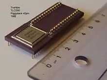
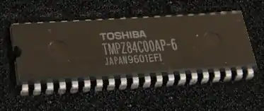
Toshiba TLCS
TLCS is a prefix applied to microcontrollers made by Toshiba. The product line includes multiple families of CISC and RISC architectures. Individual components generally have a part number beginning with "TMP". E.g. the TMP8048AP is a member of the TLCS-48 family.[1]: 11
TLCS-12
The TLCS-12 was a 12-bit microprocessor and central processing unit manufactured by Toshiba. It began development in 1971, and was completed in 1973. It was a 32 mm² MOS integrated circuit chip with about 2,800 silicon gates, fabricated on a 6 µm process with NMOS logic. It was used in the Ford EEC engine control unit system, which began production in 1974 and went into mass production in 1975. The system memory included 512-bit RAM, 2 kb ROM and 2 kb EPROM.[2][3]
TLCS-47 family
The microcontrollers in the TLCS-47 category are 4-bit systems. These are no longer advertised on the Toshiba website.
TLCS-48 family
The TLCS-48 family were clones of the Intel MCS-48 (8048) microcontroller.[1]
TLCS-90 family

The microcontrollers in the TLCS-90 family use a 8-bit/16-bit architecture reminiscent of the Z80.[1] These are no longer advertised on the Toshiba website.
The TLCS-90 inherits most Z80 features, such as:
- seven 8-bit registers (A, B, C, D, E, H and L),
- six 16-bit registers (BC, DE, HL, IX, IY, and SP), three of which are 8-bit register pairs,
- the combined parity/overflow flag,
- the
EX DE,HL,EX AF,AF'andEXX16-bit exchange instructions,[1]: Appendix-2 and - the
LDIRandLDDRmemory copy instructions.
There are, however, significant differences. It omits the separate I/O address space of the Z80, but adds more flexibility to operand combinations, some new operations (notably multiply and divide), and several additional addressing modes:
(SP+d)and(HL+A)indexed modes operating similarly to(IX+d)and(IY+d)- single-byte "zero page" addressing of memory from FF00–FFFF16
(IX)and(IY)addressing without a displacement, enabling a single byte of machine code to be saved and the execution time to be increased- PC-relative long (-32768 to +32767 bytes from the program counter, rather than the shorter -128 to +127)
Most of the functionality of 8-bit accumulator A has also been implemented for the 16-bit HL register pair, such as the missing SUB and CP instructions, and the AND, XOR, and OR bitwise instructions. The ADD HL,rr flag quirk from the Z80 is implemented. Furthermore, the DJNZ BC,addrinstruction was added to ease 16-bit loop counting.
TLCS-90 SoC packages include the 4-bit BX and BY registers, which get concatenated with effective addresses based on the IX or IY register, allowing the processor to address up to one megabyte of memory.[1]: MPU90-16 The processor includes the INCX ($FF00+n) and DECX ($FF00+n) instructions, which are useful for performing 20-bit pointer arithmetic using the IX and BX registers or the IY and BY registers.
Instructions are divided into one-byte basic and two-byte extended instructions. Opcodes E016 through FE16 are prefixes which begin an extended instruction. The instruction encoding is unusual in that the prefix specifies one operand of the extended instruction, and unlike the single-byte prefixes used by the Z80 or x86 architecture, may itself be followed by operand bytes.[1]: MPU90-23,Appendix-12 After the prefix bytes, the second opcode byte specifies the operation and second operand.
For example, the instruction ADD (IX+127),5 is encoded as F4 7F 68 05, where the first two bytes specify the destination address, the third byte specifies the operation, and the fourth byte provides the source operand.
TLCS-870 family
The microcontrollers in the TLCS-870 family (TLCS-870, TLCS-870/X, TLCS-870/C and TLCS-870/C1 series) use a 8-bit/16-bit architecture inspired by the TLCS-90, but less like the Z80.
The TLCS-870 is the original, with a 16-bit address space, which was extended in two different directions:
- TLCS-870/X extends the architecture to 20 bits in an upward-compatible way.[4]
- TLCS-870/C retains the 16-bit address space, and provides a compatible assembly language, but changes the instruction encoding[4] so that a different object code is required.
- TLCS-870/C1 is an upward-compatible variant of the 870/C with minor extensions.[5]
TLCS-900 family
The TLCS-900 family inherits most features from the TLCS-90 architecture, and includes 32-bit registers and a 24-bit address bus. Most implementations (TLCS-900,[6] TLCS-900/L,[6] TLCS-900/H and TLCS-900/L1 series) have 16-bit internal data paths, like the MC68000, while the TLCS-900/H1 series is 32 bits wide internally (like the MC68020).
The instruction set is mostly upward-compatible with the TLCS-90, although the binary encoding differs.[6]: 182–184 The same scheme of encoding the addressing mode before the instruction's opcode and additional operands is implemented. The early models supported both a "minimum mode" where the banked registers and program counter were 16 bits wide, and a "maximum mode" which had all 32-bit general purpose registers. Later models omitted the minimum mode.
In maximum mode, there are 4 banks of four 32-bit registers, each of which can be split into two 16-bit halves or four 8-bit quarters. In the minimum mode of early models, there are 8 banks of four 16-bit registers, which can be split into 8-bit halves. The processor can use the current bank (pointed to by the RFP field in the 16-bit status register SR), the previous bank to be compatible with the alternate register scheme of the TLCS-90, or any arbitrary bank number from 0 to 7. There is also a fixed set of four 32-bit registers, with one of them dedicated as the stack pointer. Early models had two separate stack pointers for user and system modes. Normally, only a set of 8 registers can be addressed from a 3-bit code; addressing all registers requires an additional 6/8-bit code byte that can only be inserted in the prefixed addressing mode operand, restricting which combinations of registers can be used for the source and destination operands.[6]
The F register (low 8-bit half of the 16-bit register SR) has an alternate register called F'. Executing EX AF,AF' from the TLCS-90 requires executing both EX A,A' and EX F,F'.
The TLCS-900 also includes 4 "microDMA" transfer channels, each of which have programmable source and destination addresses, transfer counts, data sizes (byte, word, and longword), and various transfer modes. These are triggered the same way as normal interrupts, and interrupt program execution upon the transferring process.
The TLCS-900/H model was most prominently used in the Neo Geo Pocket and Neo Geo Pocket Color.
Features and differences
Current TLCS processors offer some or all of the following features:
- multifunction, bi-directional general purpose I/O ports with optional built-in pull-up resistors
- mask programmable, one time programmable, flash memory or EEPROM type of ROM. ROMless versions are also available
- a variety of serial interfaces:
- watchdog timer (WDT)
- multiplexed 10-bit A/D converters; D/A converters
- dual clock inputs and on-line clock switching by selecting different gear values (frequency divider), thus allowing either low-power low-frequency modes or high-performance high-frequency modes
- prescalable 8-bit and 16-bit timers (may be used as Programmable Interval Timers)
- 8-bit and 16-bit pulse-width modulation (PWM) and programmable pulse generation (PPG) output
- power voltage supply range between 1.8 and 5.5 Volt
- external interrupt control
- pattern generator, suitable for stepper motor control
- Chip select/wait controller
- different chip carrier formats
As demand for these features differs widely depending on the requirements for a specific project (low energy consumption; high number of I/O ports; etc.), customers can choose from a wide range of different versions.
Development tools
Toshiba offers an ANSI C compatible C compiler and an assembler. Neither tool is available for free.
The free Small Device C Compiler supports the TLCS-90.
There is a project for porting GNU assembler to the TLCS-900 family.
Alfred Arnold's The Macroassembler AS is a free assembler supporting the TLCS-47, TLCS-870, TLCS-90, TLCS-900 and TLCS-9000 families.
References
- 8-Bit Microcontroller: TLCS-48, -90 (PDF). Toshiba. November 1988. Archived (PDF) from the original on 2020-03-28. Alt URL
- "1973: 12-bit engine-control microprocessor (Toshiba)" (PDF). Semiconductor History Museum of Japan. Retrieved 27 June 2019.
- Belzer, Jack; Holzman, Albert G.; Kent, Allen (1978). Encyclopedia of Computer Science and Technology: Volume 10 - Linear and Matrix Algebra to Microorganisms: Computer-Assisted Identification. CRC Press. p. 402. ISBN 9780824722609.
- Haywood, David. "MAME soure code: src/devices/cpu/tlcs870/tlcs870d.cpp". GitHub. Retrieved 25 April 2020.
- "TLCS-870/C1 Series Instruction Set" (PDF). Toshiba Corporation Semiconductor Company. 16 December 2008.
- "TLCS-900 Series 16-bit Microcontroller User's Manual" (PDF). Toshiba corporation. 1994 – via Bitsavers.org.
