Xenon (processor)
Microsoft XCPU, codenamed Xenon, is a CPU used in the Xbox 360 game console, to be used with ATI's Xenos graphics chip.
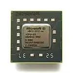 Picture of the microprocessor (XCPU-ES shown). | |
| General information | |
|---|---|
| Designed by | IBM |
| Common manufacturer(s) | |
| Cache | |
| L1 cache | 32/32 KB |
| L2 cache | 1 MB |
| Architecture and classification | |
| Instruction set | PowerPC |
| Physical specifications | |
| Cores |
|
| POWER, PowerPC, and Power ISA architectures |
|---|
| NXP (formerly Freescale and Motorola) |
| IBM |
|
| IBM/Nintendo |
| Other |
| Related links |
| Cancelled in gray, historic in italic |
The processor was developed by Microsoft and IBM under the IBM chip program codenamed "Waternoose", which was named after the Monsters, Inc. character Henry J. Waternoose III.[1] The development program was originally announced on November 3, 2003.[2]
The processor is based on IBM PowerPC instruction set architecture. It consists of three independent processor cores on a single die. These cores are slightly modified versions of the PPE in the Cell processor used on the PlayStation 3.[3][4] Each core has two symmetric hardware threads (SMT), for a total of six hardware threads available to games. Each individual core also includes 32 KB of L1 instruction cache and 32 KB of L1 data cache.
The XCPU processors were manufactured at IBM's East Fishkill, New York fabrication plant and Chartered Semiconductor Manufacturing (now part of GlobalFoundries) in Singapore.[5] Chartered reduced the fabrication process in 2007 to 65 nm from 90 nm, thus reducing manufacturing costs for Microsoft.
Specifications
- 90 nm process,[6] 65 nm process upgrade in 2007[7] (codenamed "Loki"), 45 nm process since Xbox 360 S model[8]
- 165 million transistors
- Three cores, each two-way SMT-capable and clocked at 3.2 GHz[6]
- SIMD: Two VMX128 units with a dedicated (128×128 bit) register file for each core,[6] one for each thread
- 1 MB L2 cache[6] (lockable by the GPU) running at half-speed (1.6 GHz) with a 256-bit bus
- 51.2 GB/s of L2 memory bandwidth (256 bit × 1600 MHz)
- 21.6 GB/s front-side bus (On the CPU side, this interfaces to a 1.35 GHz, 8B wide, FSB dataflow; on the GPU side, it connects to a 16B wide FSB dataflow running at 675 MHz.)[6]
- Dot product performance: 9.6 billion per second
- In-order instruction execution[6]
- 768 bits of IBM eFUSE-based OTP memory[9]
- ROM (and 64 KB SRAM) storing Microsoft's Secure Bootloader, and encryption hypervisor[9]
- Big-endian architecture
XCGPU
The Xbox 360 S introduced the XCGPU, which integrated the Xenon CPU and the Xenos GPU onto the same die, and the eDRAM into the same package. The XCGPU follows the trend started with the integrated EE+GS in PlayStation 2 Slimline, combining CPU, GPU, memory controllers and IO in a single cost-reduced chip. It also contains a "front side bus replacement block" that connects the CPU and GPU internally in exactly the same manner as the front side bus would have done when the CPU and GPU were separate chips, so that the XCGPU doesn't change the hardware characteristics of the Xbox 360.
XCGPU contains 372 million transistors and is manufactured by GlobalFoundries on a 45 nm process. Compared to the original chipset in the Xbox 360 the combined power requirements are reduced by 60% and the physical chip area by 50%.[10][11]
Gallery
Illustrations of the different generations of processors in Xbox 360 and Xbox 360 S.
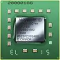 The original XCPU-ES manufactured at 90 nm by IBM in 2005. ES stands for "Engineering Sample" and the device is packaged by IBM at their Bromont facility in Canada. It runs at 2.8GHz, as opposed to the final chip, which ran at 3.2GHz.
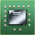 The 90nm XCPU manufactured at 90 nm by Chartered in Singapore 2006.
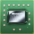 The 65nm XCPU manufactured at 65 nm by Chartered in Singapore 2007.
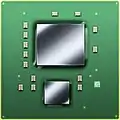 The two chips of the XCGPU: The larger is the XCGPU itself and the smaller is the 10 MB eDRAM. Manufactured at 45 nm by Global Foundries in Singapore in 2010.
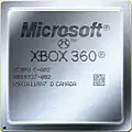 The XCGPU with heatspreader. The complete device is packaged by IBM at their Bromont facility in Canada.
References
- Takahashi, Dean (May 1, 2006). "Learning from failure - The inside story on how IBM out-foxed Intel with the Xbox 360". Electronic Business. Archived from the original on August 27, 2009.
- "IBM News room - 2003-11-03 Microsoft and IBM Announce Technology Agreement - United States". ibm.com.
- "Processing The Truth: An Interview With David Shippy", Leigh Alexander, Gamasutra, January 16, 2009
- "Playing the Fool", Jonathan V. Last, Wall Street Journal, December 30, 2008
- "IBM News room - 2005-10-25 IBM Delivers Power-based Chip for Microsoft Xbox 360 Worldwide Launch - United States". ibm.com.
- Jeffrey Brown (December 6, 2005). "Application-customized CPU design: The Microsoft Xbox 360 CPU story". IBM. Archived from the original on October 25, 2007. Retrieved September 8, 2007.
- César A. Berardini (August 21, 2006). "Chartered to Manufacture 65-nm Xbox 360 CPUs". Archived from the original on January 23, 2008. Retrieved January 9, 2008.
- Patel, Nilay (June 14, 2010). "New Xbox 360 looks angular and Ominous". Engadget.com. Retrieved June 14, 2010.
- "Xbox360 security system". YouTube. Archived from the original on December 19, 2021.
- Jon Stokes, Ars Technica (August 24, 2010). "Microsoft beats Intel, AMD to market with CPU/GPU combo chip". Retrieved August 24, 2010.
- PC Perspective (June 21, 2010). "The New Xbox 360 S "Slim" Teardown: Opened and Tested". Archived from the original on June 25, 2010. Retrieved June 24, 2010.
- Xenon hardware overview Archived February 20, 2006, at the Wayback Machine by Pete Isensee, Development Lead, Xbox Advanced Technology Group, written some time before June 23, 2007