XOR gate
XOR gate (sometimes EOR, or EXOR and pronounced as Exclusive OR) is a digital logic gate that gives a true (1 or HIGH) output when the number of true inputs is odd. An XOR gate implements an exclusive or () from mathematical logic; that is, a true output results if one, and only one, of the inputs to the gate is true. If both inputs are false (0/LOW) or both are true, a false output results. XOR represents the inequality function, i.e., the output is true if the inputs are not alike otherwise the output is false. A way to remember XOR is "must have one or the other but not both".
| XOR gate truth table | ||
|---|---|---|
| Input | Output | |
| A | B | A XOR B |
| 0 | 0 | 0 |
| 0 | 1 | 1 |
| 1 | 0 | 1 |
| 1 | 1 | 0 |
An XOR gate may serve as a "programmable inverter" in which one input determines whether to invert the other input, or to simply pass it along with no change. Hence it functions as a inverter (a NOT gate) which may be activated or deactivated by a switch.[1][2]
XOR can also be viewed as addition modulo 2. As a result, XOR gates are used to implement binary addition in computers. A half adder consists of an XOR gate and an AND gate. The gate is also used in subtractors and comparators.[3]
The algebraic expressions or or all represent the XOR gate with inputs A and B. The behavior of XOR is summarized in the truth table shown on the right.
Symbols
There are three schematic symbols for XOR gates: the traditional ANSI and DIN symbols and the IEC symbol. In some cases, the DIN symbol is used with ⊕ instead of ≢. For more information see Logic Gate Symbols.
The "=1" on the IEC symbol indicates that the output is activated by only one active input.
 |
 |
 | ||
| ANSI XOR Schematic Symbol | IEC XOR Schematic Symbol | DIN XOR Schematic Symbol |
The logic symbols ⊕, Jpq, and ⊻ can be used to denote an XOR operation in algebraic expressions.
C-like languages use the caret symbol ^ to denote bitwise XOR. (Note that the caret does not denote logical conjunction (AND) in these languages, despite the similarity of symbol.)
Implementation
The XOR gate is most commonly implemented using MOSFETs circuits. Some of those implementations include:
CMOS
The Complementary metal–oxide–semiconductor (CMOS) implementation of the XOR gate.

The nMOS and pMOS transistors are arranged so that the input pairs and activate the 2 pMOS transistors of the top left or the 2 pMOS transistors of the top right respectively, connecting Vdd to the output for a logic high. The remaining input pairs and activate each one of the two nMOS paths in the bottom to Vss for a logic low.[4]
This is a twelve transistor implementation since two additional inverters with two gates each, not shown in the diagram, are needed to generate and .
Transmission gates
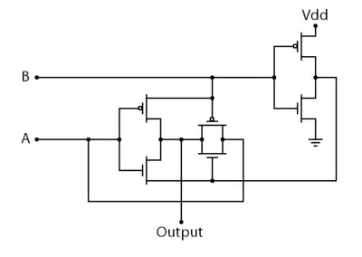
The XOR gate can also be implemented by the use of Transmission gates with pass transistor logic.

This implementation uses two Transmission gates and two inverters not shown in the diagram to generate and for a total of eight transistors, four less than in the previous design. The XOR function is implemented by passing through to the output the inverted value of A when B is high and passing the value of A when B is at a logic low. so when both inputs are low the transmission gate at the bottom is off and the one at the top is on and lets A through which is low so the output is low. When both are high only the one at the bottom is active and lets the inverted value of A through and since A is high the output will again be low. Similarly if B stays high but A is low the output would be which is high as expected and if B is low but A is high the value of A passes through and the output is high completing the truth table for the XOR gate.[5]
The trade-off with the previous implementation is that since transmission gates are not ideal switches, there is resistance associated with them, so depending on the signal strength of the input, cascading them may degrade the output levels.[6]
Optimized pass-gate-logic wiring
The previous transmission gate implementation can be further optimized from eight to six transistors by implementing the functionality of the inverter that generates and the bottom pass-gate with just two transistors arranged like an inverter but with the source of the pMOS connected to instead of Vdd and the source of the nMOS connected to instead of GND.[6]

The two leftmost transistors mentioned above, perform an optimized conditional inversion of A when B is at a logic high using pass transistor logic to reduce the transistor count and when B is at a logic low, their output is at a high impedance state. The two in the middle are a transmission gate that drives the output to the value of A when B is at a logic low and the two rightmost transistors form an inverter needed to generate used by the transmission gate and the pass transistor logic circuit.[7]
As with the previous implementation, the direct connection of the inputs to the outputs through the pass gate transistors or thru the two leftmost transistors, should be taken into account, specially when cascading them.[6]
Alternatives

If a specific type of gate is not available, a circuit that implements the same function can be constructed from other available gates. A circuit implementing an XOR function can be trivially constructed from an XNOR gate followed by a NOT gate. If we consider the expression , we can construct an XOR gate circuit directly using AND, OR and NOT gates. However, this approach requires five gates of three different kinds.
As alternative, if different gates are available we can apply Boolean algebra to transform as stated above, and apply de Morgan's Law to the last term to get which can be implemented using only three gates as shown on the right. intuitively, XOR is equivalent to OR except for when both A and B are high. So the AND of the OR with then NAND that gives a low only when both A and B are high is equivalent to the XOR.
An XOR gate circuit can be made from four NAND gates. In fact, both NAND and NOR gates are so-called "universal gates" and any logical function can be constructed from either NAND logic or NOR logic alone. If the four NAND gates are replaced by NOR gates, this results in an XNOR gate, which can be converted to an XOR gate by inverting the output or one of the inputs (e.g. with a fifth NOR gate).
| Desired gate | NAND construction | NOR construction |
|---|---|---|
 |  |  |
An alternative arrangement is of five NOR gates in a topology that emphasizes the construction of the function from , noting from de Morgan's Law that a NOR gate is an inverted-input AND gate. Another alternative arrangement is of five NAND gates in a topology that emphasizes the construction of the function from , noting from de Morgan's Law that a NAND gate is an inverted-input OR gate.
| Desired gate | NAND construction | NOR construction |
|---|---|---|
 |  |  |
For the NAND constructions, the upper arrangement requires fewer gates. For the NOR constructions, the lower arrangement offers the advantage of a shorter propagation delay (the time delay between an input changing and the output changing).
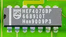
Standard chip packages

XOR chips are readily available. The most common standard chip codes are:
More than two inputs
Literal interpretation of the name "exclusive or", or observation of the IEC rectangular symbol, raises the question of correct behaviour with additional inputs.[10] If a logic gate were to accept three or more inputs and produce a true output if exactly one of those inputs were true, then it would in effect be a one-hot detector (and indeed this is the case for only two inputs). However, it is rarely implemented this way in practice.
It is most common to regard subsequent inputs as being applied through a cascade of binary exclusive-or operations: the first two signals are fed into an XOR gate, then the output of that gate is fed into a second XOR gate together with the third signal, and so on for any remaining signals. The result is a circuit that outputs a 1 when the number of 1s at its inputs is odd, and a 0 when the number of incoming 1s is even. This makes it practically useful as a parity generator or a modulo-2 adder.
For example, the 74LVC1G386 microchip is advertised as a three-input logic gate, and implements a parity generator.[11]
Applications


XOR gates and AND gates are the two most-used structures in VLSI applications.[12]
Uses in addition
The XOR logic gate can be used as a one-bit adder that adds any two bits together to output one bit. For example, if we add 1 plus 1 in binary, we expect a two-bit answer, 10 (i.e. 2 in decimal). Since the trailing sum bit in this output is achieved with XOR, the preceding carry bit is calculated with an AND gate. This is the main principle in Half Adders. A slightly larger Full Adder circuit may be chained together in order to add longer binary numbers.
In certain situations, the inputs to an OR gate (for example, in a full-adder) or to an XOR gate can never be both 1's. As this is the only combination for which the OR and XOR gate outputs differ, an OR gate may be replaced by an XOR gate (or vice versa) without altering the resulting logic. This is convenient if the circuit is being implemented using simple integrated circuit chips which contain only one gate type per chip.
Pseudo-random number generator
Pseudo-random number (PRN) generators, specifically linear-feedback shift registers (LFSR), are defined in terms of the exclusive-or operation. Hence, a suitable setup of XOR gates can model a linear-feedback shift register, in order to generate random numbers.
Correlation and sequence detection
XOR gates produce a 0 when both inputs match. When searching for a specific bit pattern or PRN sequence in a very long data sequence, a series of XOR gates can be used to compare a string of bits from the data sequence against the target sequence in parallel. The number of 0 outputs can then be counted to determine how well the data sequence matches the target sequence. Correlators are used in many communications devices such as CDMA receivers and decoders for error correction and channel codes. In a CDMA receiver, correlators are used to extract the polarity of a specific PRN sequence out of a combined collection of PRN sequences.
A correlator looking for 11010 in the data sequence 1110100101 would compare the incoming data bits against the target sequence at every possible offset while counting the number of matches (zeros):
1110100101 (data)
11010      (target)
00111      (XOR) 2 zero bits

1110100101
 11010
 00000     5 zero bits

1110100101
  11010
  01110    2 zero bits

1110100101
   11010
   10011   2 zero bits

1110100101
    11010
    01000  4 zero bits

1110100101
     11010
     11111 0 zero bits

Matches by offset:

  .
  :     :
: : : : :
-----------
0 1 2 3 4 5
In this example, the best match occurs when the target sequence is offset by 1 bit and all five bits match. When offset by 5 bits, the sequence exactly matches its inverse. By looking at the difference between the number of ones and zeros that come out of the bank of XOR gates, it is easy to see where the sequence occurs and whether or not it is inverted. Longer sequences are easier to detect than short sequences.
Phase detectors
XOR gates may be used in simplest phase detectors.[13]: 425
Analytical representation
is an analytical representation of XOR gate:
is an alternative analytical representation.
See also
- Exclusive or
- AND gate
- OR gate
- Inverter (NOT gate)
- NAND gate
- NOR gate
- XNOR gate
- IMPLY gate
- Boolean algebra
- Logic gate
References
- Broesch, James D. (2012). Practical Programmable Circuits: A Guide to PLDs, State Machines, and Microcontrollers. Elsevier Science. p. 20. ISBN 978-0323139267.
- Van Houtven, Laurens (2017). Crypto 101 (PDF). p. 17.
- Fletcher, William (1980). An engineering approach to digital design. Prentice-Hall. p. 98. ISBN 0-13-277699-5.
- Pedroni, Volnei A. (25 January 2008). Digital Electronics and Design with VHDL. Morgan Kaufmann. ISBN 978-0-08-055755-7. Retrieved 8 November 2022.
- Oklobdzija, Vojin G. (26 December 2001). The Computer Engineering Handbook. CRC Press. ISBN 978-0-8493-0885-7. Retrieved 8 November 2022.
- Designing combinational logic gates in CMOS (PDF). p. 233. Retrieved 9 November 2022.
- Annaratone, Silvia (6 December 2012). Digital CMOS Circuit Design. Springer Science & Business Media. ISBN 978-1-4613-2285-6. Retrieved 8 November 2022.
- Ferdjallah, Mohammed (15 June 2011). Introduction to Digital Systems: Modeling, Synthesis, and Simulation Using VHDL. John Wiley & Sons. p. 38. ISBN 978-1-118-00770-9. Retrieved 9 November 2022.
- Ross, Dickon; Lowe, Doug (24 September 2013). Electronics All-in-One For Dummies - UK. John Wiley & Sons. p. 647. ISBN 978-1-118-58971-7. Retrieved 9 November 2022.
- https://www.edn.com/the-xor-versus-sum-modulo-2
- 74LVC1G386 Archived 2009-12-29 at the Wayback Machine data sheet
- "Comparison of different design techniques of XOR & AND gate using EDA simulation tool".
XOR & AND gates are most important basic building blocks of any VLSI applications.
- Rabaey, Jan M. (1996). Digital integrated circuits : a design perspective. Upper Saddle River, N.J.: Prentice-Hall. ISBN 978-0-13-178609-7.
