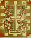
Semiconductor device fabrication
Semiconductor device fabrication is the process used to manufacture semiconductor devices, typically integrated circuit (IC) chips such as modern computer processors, microcontrollers, and memory chips such as NAND flash and DRAM that are present in everyday electrical and electronic devices. It is a multiple-step sequence of photolithographic and chemical processing steps (such as surface passivation, thermal oxidation, planar diffusion and junction isolation) during which electronic circuits are gradually created on a wafer made of pure semiconducting material. Silicon is almost always used, but various compound semiconductors are used for specialized applications.
| Semiconductor device fabrication |
|---|
 |
|
MOSFET scaling (process nodes) |
|
|
Future
|
|

| External image | |
|---|---|
The entire manufacturing process takes time, from start to packaged chips ready for shipment, at least six to eight weeks (tape-out only, not including the circuit design) and is performed in highly specialized semiconductor fabrication plants, also called foundries or fabs.[1] All fabrication takes place inside a clean room, which is the central part of a fab. In more advanced semiconductor devices, such as modern 14/10/7 nm nodes, fabrication can take up to 15 weeks, with 11–13 weeks being the industry average.[2] Production in advanced fabrication facilities is completely automated and carried out in a hermetically sealed nitrogen environment to improve yield (the percent of microchips that function correctly in a wafer), with automated material handling systems taking care of the transport of wafers from machine to machine. Wafers are transported inside FOUPs, special sealed plastic boxes. All machinery and FOUPs contain an internal nitrogen atmosphere. The air inside the machinery and FOUPs is usually kept cleaner than the surrounding air in the cleanroom. This internal atmosphere is known as a mini-environment.[3] Fabrication plants need large amounts of liquid nitrogen to maintain the atmosphere inside production machinery and FOUPs, which is constantly purged with nitrogen.[4]
Size
A specific semiconductor process has specific rules on the minimum size and spacing for features on each layer of the chip.[5] Often a newer semiconductor processes has smaller minimum sizes and tighter spacing which allow a simple die shrink to reduce costs and improve performance.[5] partly due to an increase in transistor density (number of transistors per square millimeter). Early semiconductor processes had arbitrary names such as HMOS III, CHMOS V; later ones are referred to by size such as 90 nm process.
By industry standard, each generation of the semiconductor manufacturing process, also known as technology node[6] or process node,[7][8] is designated by the process’s minimum feature size. Technology nodes, also known as "process technologies" or simply "nodes", are typically indicated by the size in nanometers (or historically micrometers) of the process' transistor gate length. However, this has not been the case since 1994. Initially transistor gate length was smaller than that suggested by the process node name (e.g. 350 nm node); however this trend reversed in 2009.[9] The nanometers used to name process nodes has become more of a marketing term that has no relation with actual feature sizes nor transistor density (number of transistors per square millimeter). For example, Intel's former 10 nm process actually has features (the tips of FinFET fins) with a width of 7 nm, Intel's former 10 nm process is similar in transistor density to TSMC's 7 nm processes, while GlobalFoundries' 12 and 14 nm processes have similar feature sizes.[10][11][12]
History
20th century
An improved type of MOSFET technology, CMOS, was developed by Chih-Tang Sah and Frank Wanlass at Fairchild Semiconductor in 1963.[13][14] CMOS was commercialised by RCA in the late 1960s.[13] RCA commercially used CMOS for its 4000-series integrated circuits in 1968, starting with a 20 µm process before gradually scaling to a 10 µm process over the next several years.[15]
Semiconductor device manufacturing has since spread from Texas and California in the 1960s to the rest of the world, including Asia, Europe, and the Middle East.
21st century
The semiconductor industry is a global business today. The leading semiconductor manufacturers typically have facilities all over the world. Samsung Electronics, the world's largest manufacturer of semiconductors, has facilities in South Korea and the US. Intel, the second-largest manufacturer, has facilities in Europe and Asia as well as the US. TSMC, the world's largest pure play foundry, has facilities in Taiwan, China, Singapore, and the US. Qualcomm and Broadcom are among the biggest fabless semiconductor companies, outsourcing their production to companies like TSMC.[16] They also have facilities spread in different countries.
Since 2009, "node" has become a commercial name for marketing purposes that indicates new generations of process technologies, without any relation to gate length, metal pitch or gate pitch.[17][18][19] For example, GlobalFoundries' 7 nm process is similar to Intel's 10 nm process, thus the conventional notion of a process node has become blurred.[20] Additionally, TSMC and Samsung's 10 nm processes are only slightly denser than Intel's 14 nm in transistor density. They are actually much closer to Intel's 14 nm process than they are to Intel's 10 nm process (e.g. Samsung's 10 nm processes' fin pitch is the exact same as that of Intel's 14 nm process: 42 nm).[21][22]
As of 2019, 14 nanometer and 10 nanometer chips are in mass production by Intel, UMC, TSMC, Samsung, Micron, SK Hynix, Toshiba Memory and GlobalFoundries, with 7 nanometer process chips in mass production by TSMC and Samsung, although their 7 nanometer node definition is similar to Intel's 10 nanometer process. The 5 nanometer process began being produced by Samsung in 2018.[23] As of 2019, the node with the highest transistor density is TSMC's 5 nanometer N5 node,[24] with a density of 171.3 million transistors per square millimeter.[25] In 2019, Samsung and TSMC announced plans to produce 3 nanometer nodes. GlobalFoundries has decided to stop the development of new nodes beyond 12 nanometers in order to save resources, as it has determined that setting up a new fab to handle sub-12 nm orders would be beyond the company's financial abilities.[26] As of 2019, Samsung is the industry leader in advanced semiconductor scaling, followed by TSMC and then Intel.[27]
List of steps
This is a list of processing techniques that are employed numerous times throughout the construction of a modern electronic device; this list does not necessarily imply a specific order. Equipment for carrying out these processes is made by a handful of companies. All equipment needs to be tested before a semiconductor fabrication plant is started.[28] These processes are done after integrated circuit design.
- Wafer processing
- Wet cleans
- Cleaning by solvents such as acetone, trichloroethylene and ultrapure water
- Piranha solution
- RCA clean
- Surface passivation
- Photolithography
- Ion implantation (in which dopants are embedded in the wafer creating regions of increased or decreased conductivity)
- Etching (microfabrication)
- Dry etching (Plasma etching)
- Reactive-ion etching (RIE)
- Deep reactive-ion etching
- Atomic layer etching (ALE)
- Reactive-ion etching (RIE)
- Wet etching
- Buffered oxide etch
- Dry etching (Plasma etching)
- Plasma ashing
- Thermal treatments
- Rapid thermal anneal
- Furnace anneals
- Thermal oxidation
- Chemical vapor deposition (CVD)
- Atomic layer deposition (ALD)
- Physical vapor deposition (PVD)
- Molecular beam epitaxy (MBE)
- Laser lift-off (for LED production[29])
- Electrochemical deposition (ECD). See Electroplating
- Chemical-mechanical polishing (CMP)
- Wafer testing (where the electrical performance is verified using Automatic Test Equipment, binning and/or laser trimming may also be carried out at this step)
- Wet cleans
- Die preparation
- Through-silicon via manufacture (For three-dimensional integrated circuits)
- Wafer mounting (wafer is mounted onto a metal frame using Dicing tape)
- Wafer backgrinding and polishing[30] (reduces the thickness of the wafer for thin devices like a smartcard or PCMCIA card or wafer bonding and stacking, this can also occur during wafer dicing, in a process known as Dice Before Grind or DBG[31][32])
- Wafer bonding and stacking (For Three-dimensional integrated circuits and MEMS)
- Redistribution layer manufacture (for WLCSP packages)
- Wafer Bumping (For Flip chip BGA (Ball grid array), and WLCSP packages)
- Die cutting or Wafer dicing
- IC packaging
- Die attachment (The die is attached to a leadframe using conductive paste or die attach film[33][34])
- IC bonding: Wire bonding, Thermosonic bonding, Flip chip or Tape Automated Bonding (TAB)
- IC encapsulation or integrated heat spreader (IHS) installation
- Molding (using special Molding compound that may contain glass powder as filler)
- Baking
- Electroplating (plates the copper leads of the lead frames with tin to make soldering easier)
- Laser marking or silkscreen printing
- Trim and form (separates the lead frames from each other, and bends the lead frame's pins so that they can be mounted on a Printed circuit board)
- IC testing
Additionally steps such as Wright etch may be carried out.

Prevention of contamination and defects
When feature widths were far greater than about 10 micrometres, semiconductor purity was not as big of an issue as it is today in device manufacturing. As devices become more integrated, cleanrooms must become even cleaner. Today, fabrication plants are pressurized with filtered air to remove even the smallest particles, which could come to rest on the wafers and contribute to defects. The ceilings of semiconductor cleanrooms have fan filter units (FFUs) at regular intervals to constantly replace and filter the air in the cleanroom; semiconductor capital equipment may also have their own FFUs. The FFUs, combined with raised floors with grills, help ensure a laminar air flow, to ensure that particles are immediately brought down to the floor and do not stay suspended in the air due to turbulence. The workers in a semiconductor fabrication facility are required to wear cleanroom suits to protect the devices from human contamination. To prevent oxidation and to increase yield, FOUPs and semiconductor capital equipment may have a hermetically sealed pure nitrogen environment with ISO class 1 level of dust. FOUPs and SMIF pods isolate the wafers from the air in the cleanroom, increasing yield because they reduce the number of defects caused by dust particles. Also, fabs have as few people as possible in the cleanroom to make maintaining the cleanroom environment easier, since people, even when wearing cleanroom suits, shed large amounts of particles, especially when walking.[35][36][37]
Wafers
A typical wafer is made out of extremely pure silicon that is grown into mono-crystalline cylindrical ingots (boules) up to 300 mm (slightly less than 12 inches) in diameter using the Czochralski process. These ingots are then sliced into wafers about 0.75 mm thick and polished to obtain a very regular and flat surface.
Processing
In semiconductor device fabrication, the various processing steps fall into four general categories: deposition, removal, patterning, and modification of electrical properties.
- Deposition is any process that grows, coats, or otherwise transfers a material onto the wafer. Available technologies include physical vapor deposition (PVD), chemical vapor deposition (CVD), electrochemical deposition (ECD), molecular beam epitaxy (MBE), and more recently, atomic layer deposition (ALD) among others. Deposition can be understood to include oxide layer formation, by thermal oxidation or, more specifically, LOCOS.
- Removal is any process that removes material from the wafer; examples include etch processes (either wet or dry) and chemical-mechanical planarization (CMP).
- Patterning is the shaping or altering of deposited materials, and is generally referred to as lithography. For example, in conventional lithography, the wafer is coated with a chemical called a photoresist; then, a machine called a stepper focuses, aligns, and moves a mask, exposing select portions of the wafer below to short-wavelength light; the exposed regions are washed away by a developer solution. After etching or other processing, the remaining photoresist is removed by "dry" plasma ashing (photoresist stripping or strip). The photoresist may also be removed using wet chemical processes that coat the wafer in a liquid to remove the photoresist.[38]
- Modification of electrical properties has historically entailed doping transistor sources and drains (originally by diffusion furnaces and later by ion implantation). These doping processes are followed by furnace annealing or, in advanced devices, by rapid thermal annealing (RTA); annealing serves to activate the implanted dopants. Modification of electrical properties now also extends to the reduction of a material's dielectric constant in low-k insulators via exposure to ultraviolet light in UV processing (UVP). Modification is frequently achieved by oxidation, which can be carried out to create semiconductor-insulator junctions, such as in the local oxidation of silicon (LOCOS) to fabricate metal oxide field effect transistors.
Modern chips have up to eleven or more metal levels produced in over 300 or more sequenced processing steps.
Front-end-of-line (FEOL) processing
FEOL processing refers to the formation of the transistors directly in the silicon. The raw wafer is engineered by the growth of an ultrapure, virtually defect-free silicon layer through epitaxy. In the most advanced logic devices, prior to the silicon epitaxy step, tricks are performed to improve the performance of the transistors to be built. One method involves introducing a straining step wherein a silicon variant such as silicon-germanium (SiGe) is deposited. Once the epitaxial silicon is deposited, the crystal lattice becomes stretched somewhat, resulting in improved electronic mobility. Another method, called silicon on insulator technology involves the insertion of an insulating layer between the raw silicon wafer and the thin layer of subsequent silicon epitaxy. This method results in the creation of transistors with reduced parasitic effects.
Gate oxide and implants
Front-end surface engineering is followed by growth of the gate dielectric (traditionally silicon dioxide), patterning of the gate, patterning of the source and drain regions, and subsequent implantation or diffusion of dopants to obtain the desired complementary electrical properties. In dynamic random-access memory (DRAM) devices, storage capacitors are also fabricated at this time, typically stacked above the access transistor (the now defunct DRAM manufacturer Qimonda implemented these capacitors with trenches etched deep into the silicon surface).
Metal layers
Once the various semiconductor devices have been created, they must be interconnected to form the desired electrical circuits. This occurs in a series of wafer processing steps collectively referred to as BEOL (not to be confused with back end of chip fabrication, which refers to the packaging and testing stages). BEOL processing involves creating metal interconnecting wires that are isolated by dielectric layers. The insulating material has traditionally been a form of SiO2 or a silicate glass, but recently new low dielectric constant materials are being used (such as silicon oxycarbide), typically providing dielectric constants around 2.7 (compared to 3.82 for SiO2), although materials with constants as low as 2.2 are being offered to chipmakers. High-κ dielectrics may instead be used.
Interconnect
Historically, the metal wires have been composed of aluminum. In this approach to wiring (often called subtractive aluminum), blanket films of aluminum are deposited first, patterned, and then etched, leaving isolated wires. Dielectric material is then deposited over the exposed wires. The various metal layers are interconnected by etching holes (called "vias") in the insulating material and then depositing tungsten in them with a CVD technique using tungsten hexafluoride; this approach is still used in the fabrication of many memory chips such as dynamic random-access memory (DRAM), because the number of interconnect levels is small (currently no more than four).
More recently, as the number of interconnect levels for logic has substantially increased due to the large number of transistors that are now interconnected in a modern microprocessor, the timing delay in the wiring has become so significant as to prompt a change in wiring material (from aluminum to copper interconnect layer) and a change in dielectric material (from silicon dioxides to newer low-K insulators). This performance enhancement also comes at a reduced cost via damascene processing, which eliminates processing steps. As the number of interconnect levels increases, planarization of the previous layers is required to ensure a flat surface prior to subsequent lithography. Without it, the levels would become increasingly crooked, extending outside the depth of focus of available lithography, and thus interfering with the ability to pattern. CMP (chemical-mechanical planarization) is the primary processing method to achieve such planarization, although dry etch back is still sometimes employed when the number of interconnect levels is no more than three. Copper interconnects use an electrically conductive barrier layer to prevent the copper from diffusing into ("poisoning") its surroundings.
Wafer test
The highly serialized nature of wafer processing has increased the demand for metrology in between the various processing steps. For example, thin film metrology based on ellipsometry or reflectometry is used to tightly control the thickness of gate oxide, as well as the thickness, refractive index, and extinction coefficient of photoresist and other coatings.[39] Wafer test metrology equipment is used to verify that the wafers haven't been damaged by previous processing steps up until testing; if too many dies on one wafer have failed, the entire wafer is scrapped to avoid the costs of further processing. Virtual metrology has been used to predict wafer properties based on statistical methods without performing the physical measurement itself.[1]
Device test
Once the front-end process has been completed, the semiconductor devices or chips are subjected to a variety of electrical tests to determine if they function properly. The percent of devices on the wafer found to perform properly is referred to as the yield. Manufacturers are typically secretive about their yields, but it can be as low as 30%, meaning that only 30% of the chips on the wafer work as intended. Process variation is one among many reasons for low yield. Testing is carried out to prevent faulty chips from being assembled into relatively expensive packages.
The yield is often but not necessarily related to device (die or chip) size. As an example, In December 2019, TSMC announced an average yield of ~80%, with a peak yield per wafer of >90% for their 5nm test chips with a die size of 17.92 mm2. The yield went down to 32.0% with an increase in die size to 100 mm2.[40]
The fab tests the chips on the wafer with an electronic tester that presses tiny probes against the chip. The machine marks each bad chip with a drop of dye. Currently, electronic dye marking is possible if wafer test data (results) are logged into a central computer database and chips are "binned" (i.e. sorted into virtual bins) according to predetermined test limits such as maximum operating frequencies/clocks, number of working (fully functional) cores per chip, etc. The resulting binning data can be graphed, or logged, on a wafer map to trace manufacturing defects and mark bad chips. This map can also be used during wafer assembly and packaging. Binning allows chips that would otherwise be rejected to be reused in lower-tier products, as is the case with GPUs and CPUs, increasing device yield, especially since very few chips are fully functional (have all cores functioning correctly, for example). eFUSEs may be used to disconnect parts of chips such as cores, either because they didn't work as intended during binning, or as part of market segmentation (using the same chip for low, mid and high-end tiers). Chips may have spare parts to allow the chip to fully pass testing even if it has several non-working parts.
Chips are also tested again after packaging, as the bond wires may be missing, or analog performance may be altered by the package. This is referred to as the "final test". Chips may also be imaged using x-rays.
Usually, the fab charges for testing time, with prices in the order of cents per second. Testing times vary from a few milliseconds to a couple of seconds, and the test software is optimized for reduced testing time. Multiple chip (multi-site) testing is also possible because many testers have the resources to perform most or all of the tests in parallel and on several chips at once.
Chips are often designed with "testability features" such as scan chains or a "built-in self-test" to speed testing and reduce testing costs. In certain designs that use specialized analog fab processes, wafers are also laser-trimmed during testing, in order to achieve tightly distributed resistance values as specified by the design.
Good designs try to test and statistically manage corners (extremes of silicon behavior caused by a high operating temperature combined with the extremes of fab processing steps). Most designs cope with at least 64 corners.
Device yield
Device yield or die yield is the number of working chips or dies on a wafer, given in percentage since the number of chips on a wafer (Die per wafer, DPW) can vary depending on the chips' size and the wafer's diameter. Yield degradation is a reduction in yield, which historically was mainly caused by dust particles, however since the 1990s, yield degradation is mainly caused by process variation, the process itself and by the tools used in chip manufacturing, although dust still remains a problem in many older fabs. Dust particles have an increasing effect on yield as feature sizes are shrunk with newer processes. Automation and the use of mini environments inside of production equipment, FOUPs and SMIFs have enabled a reduction in defects caused by dust particles. Device yield must be kept high to reduce the selling price of the working chips since working chips have to pay for those chips that failed, and to reduce the cost of wafer processing. Yield can also be affected by the design and operation of the fab.
Tight control over contaminants and the production process are necessary to increase yield. Contaminants may be chemical contaminants or be dust particles. "Killer defects" are those caused by dust particles that cause complete failure of the device (such as a transistor). There are also harmless defects. A particle needs to be 1/5 the size of a feature to cause a killer defect. So if a feature is 100 nm across, a particle only needs to be 20 nm across to cause a killer defect. Electrostatic electricity can also affect yield adversely. Chemical contaminants or impurities include heavy metals such as iron, copper, nickel, zinc, chromium, gold, mercury and silver, alkali metals such as sodium, potassium and lithium, and elements such as aluminum, magnesium, calcium, chlorine, sulfur, carbon, and fluorine. It is important for these elements to not remain in contact with the silicon, as they could reduce yield. Chemical mixtures may be used to remove these elements from the silicon; different mixtures are effective against different elements.
Several models are used to estimate yield. They are Murphy's model, Poisson's model, the binomial model, Moore's model and Seeds' model. There is no universal model; a model has to be chosen based on actual yield distribution (the location of defective chips) For example, Murphy's model assumes that yield loss occurs more at the edges of the wafer (non-working chips are concentrated on the edges of the wafer), Poisson's model assumes that defective dies are spread relatively evenly across the wafer, and Seeds's model assumes that defective dies are clustered together.[41]
Smaller dies cost less to produce (since more fit on a wafer, and wafers are processed and priced as a whole), and can help achieve higher yields since smaller dies have a lower chance of having a defect, due to their lower surface area on the wafer. However, smaller dies require smaller features to achieve the same functions of larger dies or surpass them, and smaller features require reduced process variation and increased purity (reduced contamination) to maintain high yields. Metrology tools are used to inspect the wafers during the production process and predict yield, so wafers predicted to have too many defects may be scrapped to save on processing costs.[42]
Die preparation
Once tested, a wafer is typically reduced in thickness in a process also known as "backlap",[43] "backfinish" or "wafer thinning"[44] before the wafer is scored and then broken into individual dies, a process known as wafer dicing. Only the good, unmarked chips are packaged.
Packaging
Plastic or ceramic packaging involves mounting the die, connecting the die pads to the pins on the package, and sealing the die. Tiny bondwires are used to connect the pads to the pins. In the 'old days' (1970s), wires were attached by hand, but now specialized machines perform the task. Traditionally, these wires have been composed of gold, leading to a lead frame (pronounced "leed frame") of solder-plated copper; lead is poisonous, so lead-free "lead frames" are now mandated by RoHS.
Chip scale package (CSP) is another packaging technology. A plastic dual in-line package, like most packages, is many times larger than the actual die hidden inside, whereas CSP chips are nearly the size of the die; a CSP can be constructed for each die before the wafer is diced.
The packaged chips are retested to ensure that they were not damaged during packaging and that the die-to-pin interconnect operation was performed correctly. A laser then etches the chip's name and numbers on the package.
Hazardous materials
Many toxic materials are used in the fabrication process.[45] These include:
- poisonous elemental dopants, such as arsenic, antimony, and phosphorus.
- poisonous compounds, such as arsine, phosphine, tungsten hexafluoride and silane.
- highly reactive liquids, such as hydrogen peroxide, fuming nitric acid, sulfuric acid, and hydrofluoric acid.
It is vital that workers should not be directly exposed to these dangerous substances. The high degree of automation common in the IC fabrication industry helps to reduce the risks of exposure. Most fabrication facilities employ exhaust management systems, such as wet scrubbers, combustors, heated absorber cartridges, etc., to control the risk to workers and to the environment.
See also
- Deathnium
- Glossary of microelectronics manufacturing terms
- List of semiconductor scale examples
- MOSFET
- Multigate device
- FinFET
- Semiconductor industry
- Foundry model
- Semiconductor equipment sales leaders by year
- International Technology Roadmap for Semiconductors
- Semiconductor consolidation
- Local oxidation of silicon (LOCOS)
- List of integrated circuit manufacturers
- List of semiconductor fabrication plants
- Microfabrication
- Semiconductor Equipment and Materials International (SEMI) — the semiconductor industry trade association
- SEMI font for labels on wafers
- Etch pit density
- Passivation
- Planar process
- Transistor count
References
- Neurotechnology Group, Berlin Institute of Technology, IEEE Xplore Digital Library. “Regression Methods for Virtual Metrology of Layer Thickness in Chemical Vapor Deposition Archived 2020-02-25 at the Wayback Machine.” January 17, 2014. Retrieved November 9, 2015.
- "8 Things You Should Know About Water & Semiconductors". ChinaWaterRisk.org. Archived from the original on 2017-09-10. Retrieved 2017-09-10.
- Kure, Tokuo; Hanaoka, Hideo; Sugiura, Takumi; Nakagawa, Shinya (2007). "Clean-room Technologies for the Mini-environment Age" (PDF). Hitachi Review. 56 (3): 70–74. CiteSeerX 10.1.1.493.1460. S2CID 30883737. Archived (PDF) from the original on 2021-11-01. Retrieved 2021-11-01.
- "FOUP Purge System - Fabmatics: Semiconductor Manufacturing Automation". www.fabmatics.com. Archived from the original on 2020-08-06. Retrieved 2020-01-04.
- Shirriff, Ken (June 2020). "Die shrink: How Intel scaled-down the 8086 processor". Retrieved 22 May 2022.
- "Overall Roadmap Technology Characteristics" (PDF). Semiconductor Industry Association.
- Shukla, Priyank. "A Brief History of Process Node Evolution". Design And Reuse.
- "Technology Node - WikiChip". Archived from the original on 2020-11-12. Retrieved 2020-10-20.
- Moore, Samuel K. (21 July 2020). "A Better Way To Measure Progress in Semiconductors". IEEE Spectrum: Technology, Engineering, and Science News. Retrieved 22 May 2022.
- Cutress, Ian. "Intel's 10nm Cannon Lake and Core i3-8121U Deep Dive Review". www.anandtech.com. Archived from the original on 2020-11-12. Retrieved 2020-11-07.
- "VLSI 2018: GlobalFoundries 12nm Leading-Performance, 12LP". 22 July 2018. Archived from the original on 7 April 2019. Retrieved 20 October 2020.
- Ridley, Jacob (April 29, 2020). "Intel 10nm isn't bigger than AMD 7nm, you're just measuring wrong". PC Gamer. Archived from the original on October 28, 2020. Retrieved October 21, 2020.
- "1963: Complementary MOS Circuit Configuration is Invented". Computer History Museum. Archived from the original on 23 July 2019. Retrieved 6 July 2019.
- Sah, Chih-Tang; Wanlass, Frank (February 1963). "Nanowatt logic using field-effect metal-oxide semiconductor triodes". 1963 IEEE International Solid-State Circuits Conference. Digest of Technical Papers. VI: 32–33. doi:10.1109/ISSCC.1963.1157450.
- Lojek, Bo (2007). History of Semiconductor Engineering. Springer Science & Business Media. p. 330. ISBN 9783540342588. Archived from the original on 2020-08-06. Retrieved 2019-07-21.
- "Top 10 Worldwide Semiconductor Sales Leaders - Q1 2017 - AnySilicon". AnySilicon. 2017-05-09. Archived from the original on 2017-11-06. Retrieved 2017-11-19.
- Shukla, Priyank. "A Brief History of Process Node Evolution". design-reuse.com. Archived from the original on 2019-07-09. Retrieved 2019-07-09.
- Hruska, Joel. "14nm, 7nm, 5nm: How low can CMOS go? It depends if you ask the engineers or the economists…". ExtremeTech. Archived from the original on 2019-07-09. Retrieved 2019-07-09.
- "Exclusive: Is Intel Really Starting To Lose Its Process Lead? 7nm Node Slated For Release in 2022". wccftech.com. 2016-09-10. Archived from the original on 2019-07-09. Retrieved 2019-07-09.
- "Life at 10nm. (Or is it 7nm?) And 3nm - Views on Advanced Silicon Platforms". eejournal.com. 2018-03-12. Archived from the original on 2019-07-09. Retrieved 2019-07-09.
- "10 nm lithography process - WikiChip". en.wikichip.org. Archived from the original on 2019-07-01. Retrieved 2019-08-17.
- "14 nm lithography process - WikiChip". en.wikichip.org. Archived from the original on 2019-07-01. Retrieved 2019-08-17.
- Shilov, Anton. "Samsung Completes Development of 5nm EUV Process Technology". AnandTech. Archived from the original on 2019-04-20. Retrieved 2019-05-31.
- Cheng, Godfrey (14 August 2019). "Moore's Law is not Dead". TSMC Blog. TSMC. Archived from the original on 16 August 2019. Retrieved 18 August 2019.
- Schor, David (2019-04-06). "TSMC Starts 5-Nanometer Risk Production". WikiChip Fuse. Archived from the original on 2020-05-05. Retrieved 2019-04-07.
- Cutress, Anton Shilov, Ian. "GlobalFoundries Stops All 7nm Development: Opts To Focus on Specialized Processes". www.anandtech.com. Archived from the original on 2019-10-12. Retrieved 2019-10-12.
- "Intel is "two to three years behind Samsung" in the race to 1nm silicon". PCGamesN. 20 May 2019. Archived from the original on 11 December 2019. Retrieved 11 December 2019.
- "Power outage partially halts Toshiba Memory's chip plant". Reuters. June 21, 2019. Archived from the original on December 16, 2019. Retrieved December 16, 2019 – via www.reuters.com.
- "Laser Lift-Off(LLO) Ideal for high brightness vertical LED manufacturing - Press Release - DISCO Corporation". www.disco.co.jp. Archived from the original on 2019-06-14. Retrieved 2019-05-26.
- "Product Information | Polishers - DISCO Corporation". www.disco.co.jp. Archived from the original on 2019-05-26. Retrieved 2019-05-26.
- "Product Information | DBG / Package Singulation - DISCO Corporation". www.disco.co.jp. Archived from the original on 2019-05-16. Retrieved 2019-05-26.
- "Plasma Dicing (Dice Before Grind) | Orbotech". www.orbotech.com.
- "Electro Conductive Die Attach Film(Under Development) | Nitto". www.nitto.com. Archived from the original on 2019-05-26. Retrieved 2019-05-26.
- "Die Attach Film Adhesives". www.henkel-adhesives.com. Archived from the original on 2019-05-26. Retrieved 2019-05-26.
- "The ASYST SMIF system - Integrated with the Tencor Surfscan 7200". Chip History. Archived from the original on 2020-10-16. Retrieved 2020-10-14.
- "Study into human particle shedding". www.cleanroomtechnology.com. Archived from the original on 2020-10-15. Retrieved 2020-10-14.
- "How a Chip Gets Made: Visiting GlobalFoundries". PCMag Asia. February 15, 2018. Archived from the original on October 14, 2020. Retrieved October 14, 2020.
- "Wafer Cleaning Procedures; Photoresist or Resist Stripping; Removal of Films and Particulates". www.eesemi.com. Archived from the original on 2020-10-15. Retrieved 2020-10-14.
- Löper, Philipp; Stuckelberger, Michael; Niesen, Bjoern; Werner, Jérémie; Filipič, Miha; Moon, Soo-Jin; Yum, Jun-Ho; Topič, Marko; De Wolf, Stefaan; Ballif, Christophe (2015). "Complex Refractive Index Spectra of CH3NH3PbI3 Perovskite Thin Films Determined by Spectroscopic Ellipsometry and Spectrophotometry". The Journal of Physical Chemistry Letters. 6 (1): 66–71. doi:10.1021/jz502471h. PMID 26263093. Retrieved 2021-11-16.
- Cutress, Dr Ian. "Early TSMC 5nm Test Chip Yields 80%, HVM Coming in H1 2020". www.anandtech.com. Archived from the original on 2020-05-25. Retrieved 2020-04-12.
- "Archived copy" (PDF). Archived from the original (PDF) on 2021-01-21. Retrieved 2020-10-23.
{{cite web}}: CS1 maint: archived copy as title (link) - "Archived copy" (PDF). Archived (PDF) from the original on 2020-10-25. Retrieved 2020-10-23.
{{cite web}}: CS1 maint: archived copy as title (link) - "Introduction to Semiconductor Technology" (PDF). STMicroelectronics. p. 6. Archived (PDF) from the original on 2018-04-03. Retrieved 2018-09-25.
- "Wafer Backgrind". eesemi.com. Archived from the original on 2021-01-22. Retrieved 2020-12-18.
- CNET. “Why tech pollution's going global Archived 2021-01-23 at the Wayback Machine.” April 25, 2002. Retrieved November 9, 2015.
Further reading
- Kaeslin, Hubert (2008), Digital Integrated Circuit Design, from VLSI Architectures to CMOS Fabrication, Cambridge University Press, section 14.2.
- Wiki related to Chip Technology