Zen 2
Zen 2 is a computer processor microarchitecture by AMD. It is the successor of AMD's Zen and Zen+ microarchitectures, and is fabricated on the 7 nanometer MOSFET node from TSMC. The microarchitecture powers the third generation of Ryzen processors, known as Ryzen 3000 for the mainstream desktop chips (codename "Matisse"), Ryzen 4000U/H (codename "Renoir") and Ryzen 5000U (codename "Lucienne") for mobile applications, as Threadripper 3000 for high-end desktop systems,[5][6] and as Ryzen 4000G for accelerated processing units (APUs). The Ryzen 3000 series CPUs were released on 7 July 2019,[7][8] while the Zen 2-based Epyc server CPUs (codename "Rome") were released on 7 August 2019.[9] An additional chip, the Ryzen 9 3950X, was released in November 2019.[7]
| General information | |
|---|---|
| Launched | 7 July 2019[1] |
| Designed by | AMD |
| Common manufacturer(s) |
|
| Cache | |
| L1 cache | 64 KB per core |
| L2 cache | 512 KB per core |
| Architecture and classification | |
| Technology node | TSMC 7 nm[2][3] TSMC 6 nm[4] |
| Instruction set | AMD64 (x86_64) |
| Physical specifications | |
| Cores |
|
| Socket(s) |
|
| Products, models, variants | |
| Product code name(s) |
|
| History | |
| Predecessor | Zen+ |
| Successor | Zen 3 |
At CES 2019, AMD showed a Ryzen third-generation engineering sample that contained one chiplet with eight cores and 16 threads.[5] AMD CEO Lisa Su also said to expect more than eight cores in the final lineup.[10] At Computex 2019, AMD revealed that the Zen 2 "Matisse" processors would feature up to 12 cores, and a few weeks later a 16 core processor was also revealed at E3 2019, being the aforementioned Ryzen 9 3950X.[11][12]
Zen 2 includes hardware mitigations to the Spectre security vulnerability.[13] Zen 2-based EPYC server CPUs use a design in which multiple CPU dies (up to eight in total) manufactured on a 7 nm process ("chiplets") are combined with a 14 nm I/O die on each multi-chip module (MCM) package. Using this, up to 64 physical cores and 128 total compute threads (with simultaneous multithreading) are supported per socket. This architecture is nearly identical to the layout of the "pro-consumer" flagship processor Threadripper 3990X.[14] Zen 2 delivers about 15% more instructions per clock than Zen and Zen+,[15][16] the 14- and 12-nm microarchitectures utilized on first and second generation Ryzen respectively.
Both the PlayStation 5 and the Xbox Series X and Series S use chips based on the Zen 2 microarchitecture, with proprietary tweaks and different configurations in each system's implementation than AMD sells in its own commercially available APUs.[17][18]
Design
%2540Zen2%2540Matisse%2540Ryzen_5_3600%2540100-000000031_BF_1923SUT_9HM6935R90062_DSCx2%2540Infrared.jpg.webp)
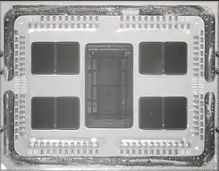
Zen 2 is a significant departure from the physical design paradigm of AMD's previous Zen architectures, Zen and Zen+. Zen 2 moves to a multi-chip module design where the I/O components of the CPU are laid out on its own, separate die, which is also called a chiplet in this context. This separation has benefits in scalability and manufacturability. As physical interfaces don't scale very well with shrinks in process technology, their separation into a different die allows these components to be manufactured using a larger, more mature process node than the CPU dies. The CPU dies (referred to by AMD as core complex dies or CCDs), now more compact due to the move of I/O components onto another die, can be manufactured using a smaller process with fewer manufacturing defects than a larger die would exhibit (since the chances of a die having a defect increases with device (die) size) while also allowing for more dies per wafer. In addition, the central I/O die can service multiple chiplets, making it easier to construct processors with a large number of cores.[14][19][20]
%2540Zen2%2540Rome%2540EPYC_7702_ES%25402S1404E2VJUG5_BB_ES_DSCx16_CCD_polysilicon%25405xLED.jpg.webp)
%2540Zen2%2540Rome%2540EPYC_7702_ES%25402S1404E2VJUG5_BB_ES_DSCx13_IOD_polysilicon%25405x.jpg.webp)
With Zen 2, each CPU chiplet houses 8 CPU cores, arranged in 2 core complexes (CCXs), each of 4 CPU cores. These chiplets are manufactured using TSMC's 7 nanometer MOSFET node and are about 74 to 80 mm2 in size.[19] The chiplet has about 3.8 billion transistors, while the 12 nm I/O die (IOD) is ~125 mm2 and has 2.09 billion transistors.[21] The amount of L3 cache has been doubled to 32 MB, with each CCX in the chiplet now having access to 16 MB of L3 compared to the 8 MB of Zen and Zen+.[22] AVX2 performance is greatly improved by an increase in execution unit width from 128-bit to 256-bit.[23] There are multiple variants of the I/O die: one manufactured on GlobalFoundries 14 nanometer process, and another manufactured using the same company's 12 nanometer process. The 14 nanometer dies have more features and are used for the EPYC Rome processors, whereas the 12 nm versions are used for consumer processors.[19] Both processes have similar feature sizes, so their transistor density is also similar.[24]
AMD's Zen 2 architecture can deliver higher performance at a lower power consumption than Intel's Cascade Lake architecture, with an example being the AMD Ryzen Threadripper 3970X running with a TDP of 140 W in ECO mode delivering higher performance than the Intel Core i9-10980XE running with a TDP of 165 W.[25]
New features
- Some new instruction set extensions: WBNOINVD, CLWB, RDPID, RDPRU, MCOMMIT. Each instruction uses its own CPUID bit.[26][27]
- Hardware mitigations against the Spectre V4 speculative store bypass vulnerability.[28]
- Zero-latency memory mirroring optimization (undocumented).[29]
Feature tables
CPUs
CPU features table
APUs
APU features table
Products
On 26 May 2019, AMD announced six Zen 2-based desktop Ryzen processors (codenamed "Matisse"). These included 6-core and 8-core variants in the Ryzen 5 and Ryzen 7 product lines, as well as a new Ryzen 9 line that includes the company's first 12-core and 16-core mainstream desktop processors. [30]
The Matisse I/O die is also used as the X570 chipset.
AMD's second generation of Epyc processors, codenamed "Rome", feature up to 64 cores, and were launched on 7 August 2019.[9]
3000 series (Matisse)
| Model | Release date and price |
Fab | Chiplets | Cores (threads) |
Core config[lower-roman 1] |
Clock rate (GHz) | Cache | Socket | PCIe lanes[lower-roman 2][lower-roman 3] |
Memory support |
TDP | |||
|---|---|---|---|---|---|---|---|---|---|---|---|---|---|---|
| Base | Boost | L1 | L2 | L3 | ||||||||||
| Entry-level | ||||||||||||||
| Ryzen 3 3100[31] | April 21, 2020 $99 |
TSMC 7FF |
1 × CCD 1 × I/OD |
4 (8) | 2 × 2 | 3.6 | 3.9 | 256 KB | 2 MB | 16 MB | AM4 | 24 (20+4) PCIe 4.0 |
DDR4-3200 dual-channel |
65 W |
| Ryzen 3 3300X[32] | April 21, 2020 $120 |
1 × 4 | 3.8 | 4.3 | ||||||||||
| Mainstream | ||||||||||||||
| Ryzen 5 3500[33] | November 15, 2019 OEM (West) Japan ¥16000[34] |
TSMC 7FF |
1 × CCD 1 × I/OD |
6 (6) | 2 × 3 | 3.6 | 4.1 | 384 KB | 3 MB | 16 MB | AM4 | 24 (20+4) PCIe 4.0 |
DDR4-3200 dual-channel |
65 W |
| Ryzen 5 3500X[35][36] | October 8, 2019 China ¥1099 |
32 MB | ||||||||||||
| Ryzen 5 3600[37] | July 7, 2019 US $199 |
6 (12) | 3.6 | 4.2 | ||||||||||
| Ryzen 5 PRO 3600[38] | September 30, 2019 OEM | |||||||||||||
| Ryzen 5 3600X[39] | July 7, 2019 US $249 |
3.8 | 4.4 | 95 W | ||||||||||
| Ryzen 5 3600XT[40] | July 7, 2020 US $249 |
4.5 | ||||||||||||
| Performance | ||||||||||||||
| Ryzen 7 PRO 3700[41] | September 30, 2019 OEM |
TSMC 7FF |
1 × CCD 1 × I/OD |
8 (16) | 2 × 4 | 3.6 | 4.4 | 512 KB | 4 MB | 32 MB | AM4 | 24 (20+4) PCIe 4.0 |
DDR4-3200 dual-channel |
65 W [lower-roman 4] |
| Ryzen 7 3700X[43] | July 7, 2019 US $329 | |||||||||||||
| Ryzen 7 3800X[44] | July 7, 2019 US $399 |
3.9 | 4.5 | 105 W | ||||||||||
| Ryzen 7 3800XT[45] | July 7, 2020 US $399 |
4.7 | ||||||||||||
| Enthusiast | ||||||||||||||
| Ryzen 9 3900[46] | October 8, 2019 OEM |
TSMC 7FF |
2 × CCD 1 × I/OD |
12 (24) | 4 × 3 | 3.1 | 4.3 | 768 KB | 6 MB | 64 MB | AM4 | 24 (20+4) PCIe 4.0 |
DDR4-3200 dual-channel |
65 W |
| Ryzen 9 PRO 3900[47] | September 30, 2019 OEM | |||||||||||||
| Ryzen 9 3900X[48] | July 7, 2019 US $499 |
3.8 | 4.6 | 105 W [lower-roman 5] | ||||||||||
| Ryzen 9 3900XT[49] | July 7, 2020 US $499 |
4.7 | ||||||||||||
| Ryzen 9 3950X[50] | November 25, 2019 US $749 |
16 (32) | 4 × 4 | 3.5 | 1 MB | 8 MB | ||||||||
| High-End Desktop (HEDT) | ||||||||||||||
| Ryzen Threadripper 3960X[51] | November 25, 2019 US $1399 |
TSMC 7FF |
4 × CCD 1 × I/OD |
24 (48) | 8 × 3 | 3.8 | 4.5 | 1.5 MB | 12 MB | 128 MB | sTRX4 | 64 (56+8) PCIe 4.0 |
DDR4-3200 quad-channel |
280 W [lower-roman 6] |
| Ryzen Threadripper 3970X[53] | November 25, 2019 US $1999 |
32 (64) | 8 × 4 | 3.7 | 4.5 | 2 MB | 16 MB | |||||||
| Ryzen Threadripper 3990X[54] | February 7, 2020 US $3990 |
8 × CCD 1 × I/OD |
64 (128) | 16 × 4 | 2.9 | 4.3 | 4 MB | 32 MB | 256 MB | |||||
| Workstation | ||||||||||||||
| Ryzen Threadripper PRO 3945WX[55] |
July 14, 2020 OEM |
TSMC 7FF |
2 × CCD 1 × I/OD |
12 (24) | 4 × 3 | 4.0 | 4.3 | 768 KB | 6 MB | 64 MB | sWRX8 | 128 (120+8) PCIe 4.0 |
DDR4-3200 octa-channel |
280 W |
| Ryzen Threadripper PRO 3955WX[56] |
July 14, 2020 OEM |
16 (32) | 4 × 4 | 3.9 | 1 MB | 8 MB | ||||||||
| Ryzen Threadripper PRO 3975WX[57] |
July 14, 2020 OEM |
4 × CCD 1 × I/OD |
32 (64) | 8 × 4 | 3.5 | 4.2 | 2 MB | 16 MB | 128 MB | |||||
| Ryzen Threadripper PRO 3995WX[58] |
July 14, 2020 OEM |
8 × CCD 1 × I/OD |
64 (128) | 16 × 4 | 2.7 | 4.2 | 4 MB | 32 MB | 256 MB | |||||
- Core Complexes (CCXs) × cores per CCX
- User accessible+Chipset link
- The chipset itself provides additional user-accessible PCIe lanes and integrated PCIe devices, see AM4 chipsets.
- Ryzen 7 3700X may consume over 90 W under load.[42]
- Ryzen 9 3900X and Ryzen 9 3950X may consume over 145 W under load.[42]
- Ryzen Threadripper 3990X may consume over 490 W under load.[52]
4000 series (Renoir)
Based on the Ryzen 4000G series APUs but with the integrated graphics disabled.
| Model | Release date and price |
Fab | Cores (threads) |
Core config[lower-roman 1] |
Clock rate (GHz) | Cache | Socket | PCIe lanes[lower-roman 2] |
Memory support |
TDP | ||||
|---|---|---|---|---|---|---|---|---|---|---|---|---|---|---|
| Base | Boost | L1 | L2 | L3 | ||||||||||
| Ryzen 3 | ||||||||||||||
| 4100[59] | April 4, 2022 US $99 |
TSMC 7FF |
4 (8) | 1 × 4 | 3.8 | 4.0 | 256 KB | 2 MB | 4 MB | AM4 | 24 (20+4) PCIe 3.0 |
DDR4-3200 dual-channel |
65 W | |
| Ryzen 5 | ||||||||||||||
| 4500[60] | April 4, 2022 US $129 |
TSMC 7FF |
6 (12) | 1 × 6 | 3.6 | 4.1 | 384 KB | 3 MB | 8 MB | AM4 | 24 (20+4) PCIe 3.0 |
DDR4-3200 dual-channel |
65 W | |
- Core Complexes (CCX) × cores per CCX
- User accessible+Chipset link
Desktop APUs
| Model | Release date and price |
Fab | CPU | GPU | Socket | PCIe lanes |
Memory support |
TDP | |||||||||
|---|---|---|---|---|---|---|---|---|---|---|---|---|---|---|---|---|---|
| Cores (threads) |
Core Config[lower-roman 1] |
Clock rate (GHz) | Cache | Archi- tecture |
Config[lower-roman 2] | Clock (GHz) |
Processing power[lower-roman 3] (GFLOPS) | ||||||||||
| Base | Boost | L1 | L2 | L3 | |||||||||||||
| Ryzen 3 | |||||||||||||||||
| 4300GE[note 1][61] | July 21, 2020 (OEM only) |
TSMC 7FF |
4 (8) | 1 × 4 | 3.5 | 4.0 | 32 KB inst. 32 KB data per core |
512 KB per core |
4 MB | GCN 5th gen |
384:24:12 6 CU |
1.7 | 1305.6 | AM4 | 24 (20+4) PCIe 3.0 |
DDR4-3200 dual-channel |
35 W |
| 4300G[note 1][62] | 3.8 | 65 W | |||||||||||||||
| Ryzen 5 | |||||||||||||||||
| 4600GE[note 1][63] | July 21, 2020 (OEM only) |
TSMC 7FF |
6 (12) | 2 × 3 | 3.3 | 4.2 | 32 KB inst. 32 KB data per core |
512 KB per core |
8 MB | GCN 5th gen |
448:28:14 7 CU |
1.9 | 1702.4 | AM4 | 24 (20+4) PCIe 3.0 |
DDR4-3200 dual-channel |
35 W |
| 4600G[note 1][64] | April 4, 2022 US $154 |
3.7 | 65 W | ||||||||||||||
| Ryzen 7 | |||||||||||||||||
| 4700GE[note 1][65] | July 21, 2020 (OEM only) |
TSMC 7FF |
8 (16) | 2 × 4 | 3.1 | 4.3 | 32 KB inst. 32 KB data per core |
512 KB per core |
8 MB | GCN 5th gen |
512:32:16 8 CU |
2.0 | 2048 | AM4 | 24 (20+4) PCIe 3.0 |
DDR4-3200 dual-channel |
35 W |
| 4700G[note 1][66] | 3.6 | 4.4 | 2.1 | 2150.4 | 65 W | ||||||||||||
- Core complexes (CCXs) × cores per CCX
- Unified Shaders : Texture Mapping Units : Render Output Units and Compute Units (CU)
- Single-precision performance is calculated from the base (or boost) core clock speed based on a FMA operation.
- Model also available as PRO version as 4350GE,[note 2] 4350G,[note 3] 4650GE,[note 4] 4650G,[note 5] 4750GE,[note 6] 4750G,[note 7] released on July 21, 2020 for OEM only.[note 8]
- "AMD Ryzen 3 PRO 4350GE". AMD. Retrieved 18 October 2022.
- "AMD Ryzen 3 PRO 4350G". AMD. Retrieved 18 October 2022.
- "AMD Ryzen 3 PRO 4650GE". AMD. Retrieved 18 October 2022.
- "AMD Ryzen 3 PRO 4650G". AMD. Retrieved 18 October 2022.
- "AMD Ryzen 3 PRO 4750GE". AMD. Retrieved 18 October 2022.
- "AMD Ryzen 3 PRO 4750G". AMD. Retrieved 18 October 2022.
- "AMD Ryzen 4000 Series Desktop Processors with AMD Radeon Graphics Set to Deliver Breakthrough Performance for Commercial and Consumer Desktop PCs". AMD. 21 July 2020. Retrieved 18 October 2022.
Renoir (4000 series)
| Model | Release date |
Fab | CPU | GPU | Socket | PCIe lanes |
Memory support | TDP | |||||||||
|---|---|---|---|---|---|---|---|---|---|---|---|---|---|---|---|---|---|
| Cores (threads) |
Core config[lower-roman 1] | Clock rate (GHz) | Cache | Archi- tecture |
Config[lower-roman 2] | Clock | Processing power (GFLOPS)[lower-roman 3] | ||||||||||
| Base | Boost | L1 | L2 | L3 | |||||||||||||
| Ryzen 3 4300U[note 1][67][68] | March 16, 2020 | TSMC 7FF |
4 (4) | 1 × 4 | 2.7 | 3.7 | 32 KB inst. 32 KB data per core |
512 KB per core |
4 MB | GCN 5th gen |
320:20:8 5 CU |
1400 MHz | 896 | FP6 | 16 (8+4+4) PCIe 3.0 |
DDR4-3200 LPDDR4-4266 dual-channel |
10–25 W |
| Ryzen 5 4500U[69][70] | 6 (6) | 2 × 3 | 2.3 | 4.0 | 8 MB 4 MB per CCX |
384:24:8 6 CU |
1500 MHz | 1152 | |||||||||
| Ryzen 5 4600U[note 1][71] | 6 (12) | 2.1 | |||||||||||||||
| Ryzen 5 4680U[72] | April 13, 2021 | 448:28:8 7 CU |
1344 | ||||||||||||||
| Ryzen 5 4600HS[73] | March 16, 2020 | 3.0 | 384:24:8 6 CU |
1152 | 35 W | ||||||||||||
| Ryzen 5 4600H[74][75] | 35–54 W | ||||||||||||||||
| Ryzen 7 4700U[note 1][76] | 8 (8) | 2 × 4 | 2.0 | 4.1 | 448:28:8 7 CU |
1600 MHz | 1433.6 | 10–25 W | |||||||||
| Ryzen 7 4800U[77] | 8 (16) | 1.8 | 4.2 | 512:32:8 8 CU |
1750 MHz | 1792 | |||||||||||
| Ryzen 7 4980U[78] | April 13, 2021 | 2.0 | 4.4 | 1950 MHz | 1996.8 | ||||||||||||
| Ryzen 7 4800HS[79] | March 16, 2020 | 2.9 | 4.2 | 448:28:8 7 CU |
1600 MHz | 1433.6 | 35 W | ||||||||||
| Ryzen 7 4800H[80][81] | 35–54 W | ||||||||||||||||
| Ryzen 9 4900HS[82] | 3 | 4.3 | 512:32:8 8 CU |
1750 MHz | 1792 | 35 W | |||||||||||
| Ryzen 9 4900H[83] | 3.3 | 4.4 | 35–54 W | ||||||||||||||
- Core Complexes (CCX) × cores per CCX
- Unified shaders : texture mapping units : render output units and compute units (CU)
- Single precision performance is calculated from the base (or boost) core clock speed based on a FMA operation.
- Model also available as PRO version as 4450U[note 2], 4650U[note 3], 4750U[note 4], released May 7, 2020.
- "AMD Ryzen 3 PRO 4450U". AMD.
- "AMD Ryzen 5 PRO 4650U". AMD.
- "AMD Ryzen 7 PRO 4750U". AMD.
Lucienne (5000 series)
| Model | Release date |
Fab | CPU | GPU | Socket | PCIe support |
Memory support | TDP | |||||||||
|---|---|---|---|---|---|---|---|---|---|---|---|---|---|---|---|---|---|
| Cores (threads) |
Core config[lower-roman 1] | Clock rate (GHz) | Cache | Architecture | Config[lower-roman 2] | Clock | Processing power[lower-roman 3] (GFLOPS) | ||||||||||
| Base | Boost | L1 | L2 | L3 | |||||||||||||
| Ryzen 3 5300U[84] | January 12, 2021 | TSMC 7FF |
4 (8) | 1 × 4 | 2.6 | 3.8 | 32 KB inst. 32 KB data per core |
512 KB per core |
4 MB | GCN 5th gen | 384:24:8 6 CU |
1500 MHz | 1152 | FP6 | 16 (8+4+4) PCIe 3.0 |
DDR4-3200 LPDDR4-4266 dual-channel |
10–25 W |
| Ryzen 5 5500U[85][86] | 6 (12) | 2 × 3 | 2.1 | 4.0 | 8 MB 4 MB per CCX |
448:28:8 7 CU |
1800 MHz | 1612.8 | |||||||||
| Ryzen 7 5700U[87] | 8 (16) | 2 × 4 | 1.8 | 4.3 | 512:32:8 8 CU |
1900 MHz | 1945.6 | ||||||||||
- Core Complexes (CCX) × cores per CCX
- Unified shaders : texture mapping units : render output units and compute units (CU)
- Single precision performance is calculated from the base (or boost) core clock speed based on a FMA operation.
Embedded processors
| Model | Release date |
Fab | CPU | GPU | Socket | PCIe support |
Memory support |
TDP | ||||||||
|---|---|---|---|---|---|---|---|---|---|---|---|---|---|---|---|---|
| Cores (threads) |
Clock rate (GHz) | Cache | Archi- tecture |
Config[lower-roman 1] | Clock (GHz) |
Processing power[lower-roman 2] (GFLOPS) | ||||||||||
| Base | Boost | L1 | L2 | L3 | ||||||||||||
| V2516[88][89] | November 10, 2020[90] | TSMC 7FF |
6 (12) | 2.1 | 3.95 | 32 KB inst. 32 KB data per core |
512 KB per core |
8 MB | GCN 5 | 384:24:8 6 CU |
1.5 | 1152 | FP6 | 20 (8+4+4+4) PCIe 3.0 |
DDR4-3200 dual-channel LPDDR4X-4266 quad-channel |
10-25 W |
| V2546[88][89] | 3.0 | 3.95 | 35-54 W | |||||||||||||
| V2718[88][89] | 8 (16) | 1.7 | 4.15 | 448:28:8 7 CU |
1.6 | 1433.6 | 10-25 W | |||||||||
| V2748[88][89] | 2.9 | 4.25 | 35-54 W | |||||||||||||
- Unified Shaders : Texture Mapping Units : Render Output Units and Compute Units (CU)
- Single-precision performance is calculated from the base (or boost) core clock speed based on a FMA operation.
Server processors
Common features of these CPUs:
- Codenamed "Rome"
- Zen 2 Microarchitecture
- 7 nm TSMC Process
- SP3 Socket
- The number of PCI-E lanes: 128
- Release date: August 7, 2019 except EPYC 7H12 which was released on September 18, 2019
- Memory support: eight-channel DDR4-3200
| Model | Price | Fab | Chiplets | Cores (threads) |
Core config[lower-roman 1] |
Clock rate (GHz) | Cache | Socket & configuration |
TDP | |||
|---|---|---|---|---|---|---|---|---|---|---|---|---|
| Base | Boost | L1 | L2 | L3 | ||||||||
| EPYC 7232P | US $450 | TSMC 7FF |
2 × CCD 1 × I/OD |
8 (16) | 4 × 2 | 3.1 | 3.2 | 32 KB inst. 32 KB data per core |
512 KB per core |
32 MB 8 MB per CCX |
SP3 1P |
120 W |
| EPYC 7302P | US $825 | 4 × CCD 1 × I/OD |
16 (32) | 8 × 2 | 3 | 3.3 | 128 MB 16 MB per CCX |
155 W | ||||
| EPYC 7402P | US $1250 | 24 (48) | 8 × 3 | 2.8 | 3.35 | 180 W | ||||||
| EPYC 7502P | US $2300 | 32 (64) | 8 × 4 | 2.5 | 3.35 | |||||||
| EPYC 7702P | US $4425 | 8 × CCD 1 × I/OD |
64 (128) | 16 × 4 | 2 | 3.35 | 256 MB 16 MB per CCX |
200 W | ||||
| EPYC 7252 | US $475 | 2 × CCD 1 × I/OD |
8 (16) | 4 × 2 | 3.1 | 3.2 | 64 MB 16 MB per CCX |
SP3 2P |
120 W | |||
| EPYC 7262 | US $575 | 4 × CCD 1 × I/OD |
8 × 1 | 3.2 | 3.4 | 128 MB 16 MB per CCX |
155 W | |||||
| EPYC 7272 | US $625 | 2 × CCD 1 × I/OD |
12 (24) | 4 × 3 | 2.9 | 3.2 | 64 MB 16 MB per CCX |
120 W | ||||
| EPYC 7282 | US $650 | 16 (32) | 4 × 4 | 2.8 | 3.2 | |||||||
| EPYC 7302 | US $978 | 4 × CCD 1 × I/OD |
8 × 2 | 3 | 3.3 | 128 MB 16 MB per CCX |
155 W | |||||
| EPYC 7352 | US $1350 | 24 (48) | 8 × 3 | 2.3 | 3.2 | |||||||
| EPYC 7402 | US $1783 | 8 × 3 | 2.8 | 3.35 | 180 W | |||||||
| EPYC 7452 | US $2025 | 32 (64) | 8 × 4 | 2.35 | 3.35 | 155 W | ||||||
| EPYC 7502 | US $2600 | 8 × 4 | 2.5 | 3.35 | 180 W | |||||||
| EPYC 7532 | US $3350 | 8 × CCD 1 × I/OD |
16 × 2 | 2.4 | 3.3 | 256 MB 16 MB per CCX |
200 W | |||||
| EPYC 7542 | US $3400 | 4 × CCD 1 × I/OD |
8 × 4 | 2.9 | 3.4 | 128 MB 16 MB per CCX |
225 W | |||||
| EPYC 7552 | US $4025 | 6 × CCD 1 × I/OD |
48 (96) | 12 × 4 | 2.2 | 3.3 | 192 MB 16 MB per CCX |
200 W | ||||
| EPYC 7642 | US $4775 | 8 × CCD 1 × I/OD |
16 × 3 | 2.3 | 3.3 | 256 MB 16 MB per CCX |
225 W | |||||
| EPYC 7662 | US $6150 | 64 (128) | 16 × 4 | 2 | 3.3 | 225 W | ||||||
| EPYC 7702 | US $6450 | 2 | 3.35 | 200 W | ||||||||
| EPYC 7742 | US $6950 | 2.25 | 3.4 | 225 W | ||||||||
| EPYC 7H12 | 2.6 | 3.3 | 280 W | |||||||||
| EPYC 7F32 | US $2100 | 4 × CCD 1 × I/OD |
8 (16) | 8 × 1 | 3.7 | 3.9 | 128 MB 16 MB per CCX |
180 W | ||||
| EPYC 7F52 | US $3100 | 8 × CCD 1 × I/OD |
16 (32) | 16 × 1 | 3.5 | 3.9 | 256 MB 16 MB per CCX |
240 W | ||||
| EPYC 7F72 | US $2450 | 6 × CCD 1 × I/OD |
24 (48) | 12 × 2 | 3.2 | 3.7 | 192 MB 16 MB per CCX |
240 W | ||||
- Core Complexes (CCX) × cores per CCX
Video game consoles and other embedded
- Xbox Series X and Series S
- PlayStation 5
- Steam Deck
- AMD 4700S[91]
Gallery
 AMD Ryzen 7 3700X
%2540Zen2%2540Matisse%2540Ryzen_5_3600%2540100-000000031_BF_1923SUT_9HM6935R90062_DSC04789-DSC04810_-_ZS-DMap_(48319202011).jpg.webp) Zen 2 I/O Die
Zen 2 I/O Die%2540Zen2%2540Matisse%2540Ryzen_5_3600%2540100-000000031_BF_1923SUT_9HM6935R90062_DSCx4%2540IOD_Infrared.jpg.webp) Infrared die shot of the I/O Die
Infrared die shot of the I/O Die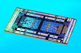 EPYC I/O Die
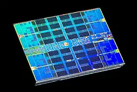 Zen 2 Core Complex Die (CCD)
%2540Zen2%2540Rome%2540EPYC_7702_ES%25402S1404E2VJUG5_BB_ES_DSCx1.jpg.webp) AMD EPYC 7702 server processor.
AMD EPYC 7702 server processor.%2540Zen2%2540Rome%2540EPYC_7702_ES%25402S1404E2VJUG5_BB_ES_DSCx3.jpg.webp) A delidded AMD 7702 featuring 8 CCDs, with remains of the solder thermal interface material (TIM) on the chiplets.
A delidded AMD 7702 featuring 8 CCDs, with remains of the solder thermal interface material (TIM) on the chiplets.
See also
- Jim Keller (engineer)
- Manycore processor
References
- "AMD Unleashes Ultimate PC Gaming Platform with Worldwide Availability of AMD Radeon RX 5700 Series Graphics Cards and AMD Ryzen 3000 Series Desktop Processors" (Press release). Santa Clara, California: Advanced Micro Devices, Inc. 7 July 2019. Retrieved 7 November 2020.
- Larabel, Michael (16 May 2017). "AMD Talks Up Vega Frontier Edition, Epyc, Zen 2, ThreadRipper". Phoronix. Retrieved 16 May 2017.
- Cutress, Ian (20 June 2017). "AMD EPYC Launch Event Live Blog". AnandTech. Retrieved 21 June 2017.
- Boshor, Gavin (20 September 2022). "AMD Launches Mendocino APUs: Zen 2-based Ryzen and Athlon 7020 Series with RDNA 2 Graphics". AnandTech. Retrieved 26 September 2022.
- Cutress, Ian (9 January 2019). "AMD Ryzen third Gen 'Matisse' Coming Mid 2019: Eight Core Zen 2 with PCIe 4.0 on Desktop". AnandTech. Retrieved 15 January 2019.
- online, heise. "AMD Ryzen 3000: 12-Kernprozessoren für den Mainstream". c't Magazin.
- Leather, Antony. "AMD Ryzen 9 3900X and Ryzen 7 3700X Review: Old Ryzen Owners Look Away Now". Forbes. Retrieved 19 September 2019.
- "AMD Ryzen 3000 CPUs launching July 7 with up to 12 cores". PCGamesN. Retrieved 28 May 2019.
- "2nd Gen AMD EPYC Processors Set New Standard for the Modern Datacenter with Record-Breaking Performance and Significant TCO Savings". AMD. 7 August 2019. Retrieved 8 August 2019.
- Hachman, Mark (9 January 2019). "AMD's CEO Lisa Su confirms ray tracing GPU development, hints at more 3rd-gen Ryzen cores". Retrieved 15 January 2019.
- Curtress, Ian (26 May 2019). "AMD Ryzen 3000 Announced: Five CPUs, 12 Cores for $499, Up to 4.6 GHz, PCIe 4.0, Coming 7/7". Retrieved 3 July 2019.
- Thomas, Bill (10 June 2019). "AMD announces the Ryzen 9 3950X, a 16-core mainstream processor". Retrieved 3 July 2019.
- Alcorn, Paul (31 January 2018). "AMD Predicts Double-Digit Revenue Growth In 2018, Ramps Up GPU Production". Tom's Hardware. Retrieved 31 January 2018.
- Shilov, Anton (6 November 2018). "AMD Unveils 'Chiplet' Design Approach: 7nm Zen 2 Cores Meet 14 nm I/O Die".
- Cutress, Ian. "AMD Zen 2 Microarchitecture Analysis: Ryzen 3000 and EPYC Rome". www.anandtech.com.
- Walton, Steven (16 November 2020). "AMD Ryzen 5000 IPC Performance Tested". TechSpot. Retrieved 18 April 2021.
- Warren, Tom (24 February 2020). "Microsoft reveals more Xbox Series X specs, confirms 12 teraflops GPU". The Verge. Retrieved 24 February 2020.
- Leadbetter, Richard (18 March 2020). "Inside PlayStation 5: the specs and the tech that deliver Sony's next-gen vision". Eurogamer. Retrieved 18 March 2020.
- Cutress, Ian (10 June 2019). "AMD Zen 2 Microarchitecture Analysis: Ryzen 3000 and EPYC Rome". AnandTech. p. 1. Retrieved 17 June 2019.
- De Gelas, Johan (7 August 2019). "AMD Rome Second Generation EPYC Review: 2x 64-core Benchmarked". AnandTech. Retrieved 29 September 2019.
- November 2019, Paul Alcorn 21 (21 November 2019). "AMD Ryzen 9 3900X and Ryzen 7 3700X Review: Zen 2 and 7nm Unleashed". Tom's Hardware.
- Cutress, Ian (10 June 2019). "AMD Zen 2 Microarchitecture Analysis: Ryzen 3000 and EPYC Rome". AnandTech. Retrieved 17 June 2019.
- Cutress, Ian (10 June 2019). "AMD Zen 2 Microarchitecture Analysis: Ryzen 3000 and EPYC Rome". AnandTech. Retrieved 17 June 2019.
- Schor, David (22 July 2018). "VLSI 2018: GlobalFoundries 12nm Leading-Performance, 12LP".
- Mujtaba, Hassan (24 December 2019). "AMD Ryzen Threadripper 3970X Is An Absolutely Efficient Monster CPU".
- "AMD Zen 2 CPUs Come With A Few New Instructions - At Least WBNOINVD, CLWB, RDPID - Phoronix". www.phoronix.com.
- "GNU Binutils Adds Bits For AMD Zen 2's RDPRU + MCOMMIT Instructions - Phoronix". www.phoronix.com.
- btarunr (12 June 2019). "AMD Zen 2 has Hardware Mitigation for Spectre V4". TechPowerUp. Retrieved 18 October 2019.
- Agner, Fog. "Surprising new feature in AMD Ryzen 3000". Agner's CPU blog.
- Cutress, Ian (26 May 2019). "AMD Ryzen 3000 Announced: Five CPUs, 12 Cores for $499, Up to 4.6 GHz, PCIe 4.0, Coming 7/7". AnandTech. Retrieved 17 June 2019.
- "AMD Ryzen 3 3100 Desktop Processor". AMD.
- "AMD Ryzen 3 3300X Desktop Processor". AMD.
- "AMD Ryzen 5 3500 Processor (OEM Only)". AMD. Retrieved 3 October 2022.
- "AMD Launches Ryzen 5 3500 in Japan with 6 Cores/6 Threads for 16K Yen". Hardware Times. 17 February 2020.
- "AMD 锐龙 5 3500X 处理器 (China Only)". AMD (in Chinese). Retrieved 3 October 2022.
- Cutress, Ian (8 October 2019). "AMD Brings Ryzen 9 3900 and Ryzen 5 3500X To Life". AnandTech.
- "AMD Ryzen 5 3600 Desktop Processor". AMD.
- "AMD Ryzen 5 PRO 3600 Processor". AMD.
- "AMD Ryzen 5 3600X Processor". AMD.
- "AMD Ryzen 5 3600XT". AMD.
- "AMD Ryzen 7 PRO 3700 Processor". AMD.
- Alcorn, Paul (14 November 2019). "Tom's Hardware Ryzen 9 3950X review". Tom's Hardware. Retrieved 12 May 2020.
- "AMD Ryzen 7 3700X". AMD.
- "AMD Ryzen 7 3800X". AMD.
- "AMD Ryzen 7 3800XT". AMD.
- "AMD Ryzen 9 3900 specifications". CPU World.
- "AMD Ryzen 9 PRO 3900 Processor". AMD.
- "AMD Ryzen 9 3900X Processor". AMD.
- "AMD Ryzen 9 3900XT Processor". AMD.
- "AMD Ryzen 9 3950X Processor". AMD.
- "AMD Ryzen Threadripper 3960X Processor". AMD.
- Hill, Luke (7 February 2020). "Kitguru AMD Ryzen Threadripper 3990X CPU Review". KitGuru. Retrieved 12 May 2020.
- "AMD Ryzen Threadripper 3970X Processor". AMD.
- "AMD Ryzen Threadripper 3990X Processor". AMD.
- "AMD Ryzen Threadripper PRO 3945WX". AMD.
- "AMD Ryzen Threadripper PRO 3955WX". AMD.
- "AMD Ryzen Threadripper PRO 3975WX". AMD.
- "AMD Ryzen Threadripper PRO 3995WX". AMD.
- "AMD Ryzen 3 4100". AMD.
- "AMD Ryzen 5 4500". AMD.
- "AMD Ryzen 3 4300GE (OEM Only)". AMD. Retrieved 9 October 2022.
- "AMD Ryzen 3 4300G (OEM Only)". AMD. Retrieved 9 October 2022.
- "AMD Ryzen 5 4600GE (OEM Only)". AMD. Retrieved 9 October 2022.
- "AMD Ryzen 5 4600G". AMD.
- "AMD Ryzen 7 4700GE (OEM Only)". AMD. Retrieved 9 October 2022.
- "AMD Ryzen 7 4700G (OEM Only)". AMD. Retrieved 9 October 2022.
- "AMD Ryzen 3 4300U". AMD.
- "AMD Ryzen 3 4300U Specs". TechPowerUp. Retrieved 17 September 2021.
- "AMD Ryzen 5 4500U". AMD.
- "AMD Ryzen 5 4500U Specs". TechPowerUp. Retrieved 17 September 2021.
- "AMD Ryzen 5 4600U". AMD.
- CoveMiner. "Surface Laptop 4 processors technical overview - Surface". docs.microsoft.com. Retrieved 14 April 2021.
- "AMD Ryzen 5 4600HS". AMD.
- "AMD Ryzen 5 4600H". AMD.
- "AMD Ryzen 5 4600H Specs". TechPowerUp. Retrieved 17 September 2021.
- "AMD Ryzen 7 4700U". AMD.
- "AMD Ryzen 7 4800U". AMD.
- CoveMiner. "Surface Laptop 4 processors technical overview - Surface". docs.microsoft.com. Retrieved 14 April 2021.
- "AMD Ryzen 7 4800HS". AMD.
- "AMD Ryzen 7 4800H". AMD.
- "AMD Ryzen 7 4800H Specs". TechPowerUp. Retrieved 17 September 2021.
- "AMD Ryzen 9 4900HS". AMD.
- "AMD Ryzen 9 4900H". AMD.
- "AMD Ryzen 3 5300U". AMD.
- "AMD Ryzen 5 5500U". AMD.
- "AMD Ryzen 5 5500U Specs". TechPowerUp. Retrieved 17 September 2021.
- "AMD Ryzen 7 5700U". AMD.
- "Embedded Processor Specifications". AMD.
- "Product Brief: AMD Ryzen Embedded V2000 Processor Family" (PDF). AMD.
- "AMD Unveils AMD Ryzen Embedded V2000 Processors with Enhanced Performance and Power Efficiency". AMD.
- "AMD 4700S 8-Core Processor Desktop Kit". AMD. Retrieved 26 September 2022.