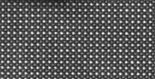
Annular dark-field imaging
Annular dark-field imaging is a method of mapping samples in a scanning transmission electron microscope (STEM). These images are formed by collecting scattered electrons with an annular dark-field detector.[1]
Conventional TEM dark-field imaging uses an objective aperture in order to only collect scattered electrons that pass through. In contrast, STEM dark-field imaging does not use an aperture to differentiate the scattered electrons from the main beam, but uses an annular detector to collect only the scattered electrons.[2] Consequently, the contrast mechanisms are different between conventional dark field imaging and STEM dark field.

An annular dark field detector collects electrons from an annulus around the beam, sampling far more scattered electrons than can pass through an objective aperture. This gives an advantage in terms of signal collection efficiency and allows the main beam to pass to an electron energy loss spectroscopy (EELS) detector, allowing both types of measurement to be performed simultaneously. Annular dark field imaging is also commonly performed in parallel with energy-dispersive X-ray spectroscopy acquisition and can be also done in parallel to bright-field (STEM) imaging.
HAADF
High-angle annular dark-field imaging (HAADF) is an STEM technique which produces an annular dark field image formed by very high angle, incoherently scattered electrons (Rutherford scattered from the nucleus of the atoms) — as opposed to Bragg scattered electrons. This technique is highly sensitive to variations in the atomic number of atoms in the sample (Z-contrast images).[3]
For elements with a higher Z, more electrons are scattered at higher angles due to greater electrostatic interactions between the nucleus and electron beam. Because of this, the HAADF detector senses a greater signal from atoms with a higher Z, causing them to appear brighter in the resulting image.[4][5]
This high dependence on Z (with contrast approximately proportional to Z2) makes HAADF a useful way to easily identify small areas of an element with a high Z in a matrix of material with a lower Z. With this in mind, a common application for HAADF is in heterogeneous catalysis research, as determination of the size of metal particles and their distribution is extremely important.
Resolution
Image resolution in HAADF STEM is very high and predominately determined by the size of the electron probe, which in turn depends on the ability to correct the aberrations of the objective lens, in particular the spherical aberration. The high resolution gives it an advantage over the detection of back scattered electrons (BSE), which can also be used to detect materials with a high Z in a matrix of material with a lower Z.
Microscope Specifications
HAADF imaging typically uses electrons scattered at an angle of >5° (Rutherford scattered electrons). For imaging on a TEM/STEM, optimum HAADF imaging is provided by TEM/STEM systems with a large maximum diffraction angle and small minimum camera length. Both of these factors allow for greater separation between Bragg and Rutherford scattered electrons.
The large maximum diffraction angle is necessary to account for materials that show Bragg scattering at high angles, such as many crystalline materials. The high maximum diffraction angle allows for good separation between Bragg and Rutherford scattered electrons, therefore it is important for the maximum diffraction angle of the microscope to be as large as possible for use with HAADF.
A small camera length is needed for the Rutherford scattered electrons to hit the detector, while avoiding the detection of Bragg scattered electrons. A small camera length will cause most of the Bragg scattered electrons to fall on the bright field detector with the transmitted electrons, leaving only the high angle scattered electrons to fall on the dark field detector.[1]
See also
References
- Otten, Max T. (1992). "High-Angle annular dark-field imaging on a tem/stem system". Journal of Electron Microscopy Technique. 17 (2): 221–230. doi:10.1002/jemt.1060170209. ISSN 0741-0581. PMID 2013823.
- Weber, Juliane (2017). Fundamental Insights into the Radium Uptake into Barite by Atom Probe Tomography and Electron Microscopy. ISBN 978-3-95806-220-7.
- DE Jesson; SJ Pennycook (1995). "Incoherent Imaging of Crystals Using Thermally Scattered Electrons". Proc. R. Soc. A. 449 (1936): 273. Bibcode:1995RSPSA.449..273J. doi:10.1098/rspa.1995.0044.
- Nellist, P.D.; Pennycook, S.J. (2000), "The principles and interpretation of annular dark-field Z-contrast imaging", Advances in Imaging and Electron Physics, Elsevier, pp. 147–203, doi:10.1016/s1076-5670(00)80013-0, ISBN 9780120147557
- "electron microscopy home". www.microscopy.ethz.ch. Archived from the original on 2018-08-14. Retrieved 2018-11-28.