Transmission electron microscopy
Transmission electron microscopy (TEM) is a microscopy technique in which a beam of electrons is transmitted through a specimen to form an image. The specimen is most often an ultrathin section less than 100 nm thick or a suspension on a grid. An image is formed from the interaction of the electrons with the sample as the beam is transmitted through the specimen. The image is then magnified and focused onto an imaging device, such as a fluorescent screen, a layer of photographic film, or a sensor such as a scintillator attached to a charge-coupled device.
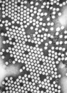
Transmission electron microscopes are capable of imaging at a significantly higher resolution than light microscopes, owing to the smaller de Broglie wavelength of electrons. This enables the instrument to capture fine detail—even as small as a single column of atoms, which is thousands of times smaller than a resolvable object seen in a light microscope. Transmission electron microscopy is a major analytical method in the physical, chemical and biological sciences. TEMs find application in cancer research, virology, and materials science as well as pollution, nanotechnology and semiconductor research, but also in other fields such as paleontology and palynology.
TEM instruments have multiple operating modes including conventional imaging, scanning TEM imaging (STEM), diffraction, spectroscopy, and combinations of these. Even within conventional imaging, there are many fundamentally different ways that contrast is produced, called "image contrast mechanisms". Contrast can arise from position-to-position differences in the thickness or density ("mass-thickness contrast"), atomic number ("Z contrast", referring to the common abbreviation Z for atomic number), crystal structure or orientation ("crystallographic contrast" or "diffraction contrast"), the slight quantum-mechanical phase shifts that individual atoms produce in electrons that pass through them ("phase contrast"), the energy lost by electrons on passing through the sample ("spectrum imaging") and more. Each mechanism tells the user a different kind of information, depending not only on the contrast mechanism but on how the microscope is used—the settings of lenses, apertures, and detectors. What this means is that a TEM is capable of returning an extraordinary variety of nanometer- and atomic-resolution information, in ideal cases revealing not only where all the atoms are but what kinds of atoms they are and how they are bonded to each other. For this reason TEM is regarded as an essential tool for nanoscience in both biological and materials fields.
The first TEM was demonstrated by Max Knoll and Ernst Ruska in 1931, with this group developing the first TEM with resolution greater than that of light in 1933 and the first commercial TEM in 1939. In 1986, Ruska was awarded the Nobel Prize in physics for the development of transmission electron microscopy.[2]
History
Initial development

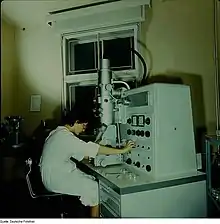
In 1873, Ernst Abbe proposed that the ability to resolve detail in an object was limited approximately by the wavelength of the light used in imaging or a few hundred nanometers for visible light microscopes. Developments in ultraviolet (UV) microscopes, led by Köhler and Rohr, increased resolving power by a factor of two.[3] However this required expensive quartz optics, due to the absorption of UV by glass. It was believed that obtaining an image with sub-micrometer information was not possible due to this wavelength constraint.[4]
In 1858, Plücker observed the deflection of "cathode rays" (electrons) by magnetic fields.[5] This effect was used by Ferdinand Braun in 1897 to build simple cathode-ray oscilloscope (CRO) measuring devices.[6] In 1891, Eduard Riecke noticed that the cathode rays could be focused by magnetic fields, allowing for simple electromagnetic lens designs. In 1926, Hans Busch published work extending this theory and showed that the lens maker's equation could, with appropriate assumptions, be applied to electrons.[2]
In 1928, at the Technical University of Berlin, Adolf Matthias, Professor of High Voltage Technology and Electrical Installations, appointed Max Knoll to lead a team of researchers to advance the CRO design. The team consisted of several PhD students including Ernst Ruska and Bodo von Borries. The research team worked on lens design and CRO column placement, to optimize parameters to construct better CROs, and make electron optical components to generate low magnification (nearly 1:1) images. In 1931, the group successfully generated magnified images of mesh grids placed over the anode aperture. The device used two magnetic lenses to achieve higher magnifications, arguably creating the first electron microscope. In that same year, Reinhold Rudenberg, the scientific director of the Siemens company, patented an electrostatic lens electron microscope.[4][7]
Improving resolution
At the time, electrons were understood to be charged particles of matter; the wave nature of electrons was not fully realized until the PhD thesis of Louis de Broglie in 1924.[8] Knoll's research group was unaware of this publication until 1932, when they realized that the de Broglie wavelength of electrons was many orders of magnitude smaller than that for light, theoretically allowing for imaging at atomic scales. (Even for electrons with a kinetic energy of just 1 electronvolt the wavelength is already as short as 1.18 nm.) In April 1932, Ruska suggested the construction of a new electron microscope for direct imaging of specimens inserted into the microscope, rather than simple mesh grids or images of apertures. With this device successful diffraction and normal imaging of an aluminium sheet was achieved. However the magnification achievable was lower than with light microscopy. Magnifications higher than those available with a light microscope were achieved in September 1933 with images of cotton fibers quickly acquired before being damaged by the electron beam.[4]
At this time, interest in the electron microscope had increased, with other groups, such as that of Paul Anderson and Kenneth Fitzsimmons of Washington State University[9] and that of Albert Prebus and James Hillier at the University of Toronto, who constructed the first TEMs in North America in 1935 and 1938, respectively,[10] continually advancing TEM design.
Research continued on the electron microscope at Siemens in 1936, where the aim of the research was the development and improvement of TEM imaging properties, particularly with regard to biological specimens. At this time electron microscopes were being fabricated for specific groups, such as the "EM1" device used at the UK National Physical Laboratory.[11] In 1939, the first commercial electron microscope, pictured, was installed in the Physics department of IG Farben-Werke. Further work on the electron microscope was hampered by the destruction of a new laboratory constructed at Siemens by an air raid, as well as the death of two of the researchers, Heinz Müller and Friedrick Krause during World War II.[12]
Further research
After World War II, Ruska resumed work at Siemens, where he continued to develop the electron microscope, producing the first microscope with 100k magnification.[12] The fundamental structure of this microscope design, with multi-stage beam preparation optics, is still used in modern microscopes. The worldwide electron microscopy community advanced with electron microscopes being manufactured in Manchester UK, the USA (RCA), Germany (Siemens) and Japan (JEOL). The first international conference in electron microscopy was in Delft in 1949, with more than one hundred attendees.[11] Later conferences included the "First" international conference in Paris, 1950 and then in London in 1954.
With the development of TEM, the associated technique of scanning transmission electron microscopy (STEM) was re-investigated and remained undeveloped until the 1970s, with Albert Crewe at the University of Chicago developing the field emission gun[13] and adding a high quality objective lens to create the modern STEM. Using this design, Crewe demonstrated the ability to image atoms using annular dark-field imaging. Crewe and coworkers at the University of Chicago developed the cold field electron emission source and built a STEM able to visualize single heavy atoms on thin carbon substrates.[14]
Background
Electrons
Theoretically, the maximum resolution, d, that one can obtain with a light microscope is limited by the wavelength of the photons (λ) and the numerical aperture NA of the system.[15]
where n is the index of refraction of the medium in which the lens is working and α is the maximum half-angle of the cone of light that can enter the lens (see numerical aperture).[16] Early twentieth century scientists theorized ways of getting around the limitations of the relatively large wavelength of visible light (wavelengths of 400–700 nanometers) by using electrons. Like all matter, electrons have both wave and particle properties (matter wave), and their wave-like properties mean that a beam of electrons can be focused and diffracted much like light can. The wavelength of electrons is related to their kinetic energy via the de Broglie equation, which says that the wavelength is inversely proportional to the momentum. Taking into account relativistic effects (as in a TEM an electron's velocity is a substantial fraction of the speed of light, c[17]) the wavelength is
where, h is Planck's constant, m0 is the rest mass of an electron and E is the kinetic energy of the accelerated electron.
Electron source
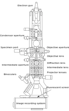
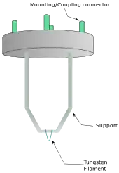
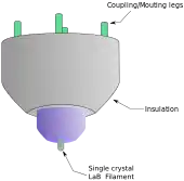
From the top down, the TEM consists of an emission source or cathode, which may be a tungsten filament, a lanthanum hexaboride (LaB6) single crystal or a field emission gun.[18] The gun is connected to a high voltage source (typically ~100–300 kV) and emits electrons either by thermionic or field electron emission into the vacuum. In the case of a thermionic source, the electron source is mounted in a Wehnelt cylinder to provide preliminary focus of the emitted electrons into a beam while also stabilizing the current using a passive feedback circuit. A field emission source uses instead electrostatic electrodes called an extractor, a suppressor, and a gun lens, with different voltages on each, to control the electric field shape and intensity near the sharp tip. The combination of the cathode and these first electrostatic lens elements is collectively called the "electron gun". After it leaves the gun, the beam is typically accelerated until it reaches its final voltage and enters the next part of the microscope: the condenser lens system. These upper lenses of the TEM then further focus the electron beam to the desired size and location on the sample.[19]
Manipulation of the electron beam is performed using two physical effects. The interaction of electrons with a magnetic field will cause electrons to move according to the left hand rule, thus allowing electromagnets to manipulate the electron beam. Additionally, electrostatic fields can cause the electrons to be deflected through a constant angle. Coupling of two deflections in opposing directions with a small intermediate gap allows for the formation of a shift in the beam path, allowing for beam shifting.
Optics
The lenses of a TEM are what gives it its flexibility of operating modes and ability to focus beams down to the atomic scale and magnify them to get an image. A lens is usually made of a solenoid coil nearly surrounded by ferromagnetic materials designed to concentrate the coil's magnetic field into a precise, confined shape. When an electron enters and leaves this magnetic field, it spirals around the curved magnetic field lines in a way that acts very much as an ordinary glass lens does for light—it is a converging lens. But, unlike a glass lens, a magnetic lens can very easily change its focusing power by adjusting the current passing through the coils.
Equally important to the lenses are the apertures. These are circular holes in thin strips of heavy metal. Some are fixed in size and position and play important roles in limiting x-ray generation and improving the vacuum performance. Others can be freely switched among several different sizes and have their positions adjusted. Variable apertures after the sample allow the user to select the range of spatial positions or electron scattering angles to be used in the formation of an image or a diffraction pattern.
The electron-optical system also includes deflectors and stigmators, usually made of small electromagnets. The deflectors allow the position and angle of the beam at the sample position to be independently controlled and also ensure that the beams remain near the low-aberration centers of every lens in the lens stacks. The stigmators compensate for slight imperfections and aberrations that cause astigmatism—a lens having a different focal strength in different directions.
Typically a TEM consists of three stages of lensing. The stages are the condenser lenses, the objective lenses, and the projector lenses. The condenser lenses are responsible for primary beam formation, while the objective lenses focus the beam that comes through the sample itself (in STEM scanning mode, there are also objective lenses above the sample to make the incident electron beam convergent). The projector lenses are used to expand the beam onto the phosphor screen or other imaging device, such as film. The magnification of the TEM is due to the ratio of the distances between the specimen and the objective lens' image plane.[20] TEM optical configurations differ significantly with implementation, with manufacturers using custom lens configurations, such as in spherical aberration corrected instruments,[19] or TEMs using energy filtering to correct electron chromatic aberration.
Reciprocity
The optical reciprocity theorem, or principle of Helmholtz reciprocity, generally holds true for elastically scattered electrons, as is often the case under standard TEM operating conditions.[21][22] The theorem states that the wave amplitude at some point B as a result of electron point source A would be the same as the amplitude at A due to an equivalent point source placed at B.[22] Simply stated, the wave function for electrons focused through any series of optical components that includes only scalar (i.e. not magnetic) fields will be exactly equivalent if the electron source and observation point are reversed. R
Reciprocity is used to understand scanning transmission electron microscopy (STEM) in the familiar context of TEM, and to obtain and interpret images using STEM.
Display and detectors
The key factors when considering electron detection include detective quantum efficiency (DQE), point spread function (PSF), modulation transfer function (MTF), pixel size and array size, noise, data readout speed, and radiation hardness.[23]
Imaging systems in a TEM consist of a phosphor screen, which may be made of fine (10–100 μm) particulate zinc sulfide, for direct observation by the operator, and an image recording system such as photographic film,[24] doped YAG screen coupled CCDs,[25] or other digital detector.[23] Typically these devices can be removed or inserted into the beam path as required. (Photograph film is no longer used.) The first report of using a Charge-Coupled Device (CCD) detector for TEM was in 1982,[26] but the technology didn't find widespread use until the late 1990s/early 2000s.[27] Monolithic active-pixel sensors (MAPSs) were also used in TEM.[28] CMOS detectors, which are faster and more resistant to radiation damage than CCDs, have been used for TEM since 2005.[29][30] In the early 2010s, further development of CMOS technology allowed for the detection of single electron counts ("counting mode").[31][32] These Direct Electron Detectors are available from Gatan, FEI, Quantum Detectors and Direct Electron.[28]
Components

A TEM is composed of several components, which include a vacuum system in which the electrons travel, an electron emission source for generation of the electron stream, a series of electromagnetic lenses, as well as electrostatic plates. The latter two allow the operator to guide and manipulate the beam as required. Also required is a device to allow the insertion into, motion within, and removal of specimens from the beam path. Imaging devices are subsequently used to create an image from the electrons that exit the system.
Vacuum system
To increase the mean free path of the electron gas interaction, a standard TEM is evacuated to low pressures, typically on the order of 10−4 Pa.[33] The need for this is twofold: first the allowance for the voltage difference between the cathode and the ground without generating an arc, and secondly to reduce the collision frequency of electrons with gas atoms to negligible levels—this effect is characterized by the mean free path. TEM components such as specimen holders and film cartridges must be routinely inserted or replaced requiring a system with the ability to re-evacuate on a regular basis. As such, TEMs are equipped with multiple pumping systems and airlocks and are not permanently vacuum sealed.
The vacuum system for evacuating a TEM to an operating pressure level consists of several stages. Initially, a low or roughing vacuum is achieved with either a rotary vane pump or diaphragm pumps setting a sufficiently low pressure to allow the operation of a turbo-molecular or diffusion pump establishing high vacuum level necessary for operations. To allow for the low vacuum pump to not require continuous operation, while continually operating the turbo-molecular pumps, the vacuum side of a low-pressure pump may be connected to chambers which accommodate the exhaust gases from the turbo-molecular pump.[34] Sections of the TEM may be isolated by the use of pressure-limiting apertures to allow for different vacuum levels in specific areas such as a higher vacuum of 10−4 to 10−7 Pa or higher in the electron gun in high-resolution or field-emission TEMs.
High-voltage TEMs require ultra-high vacuums on the range of 10−7 to 10−9 Pa to prevent the generation of an electrical arc, particularly at the TEM cathode.[35] As such for higher voltage TEMs a third vacuum system may operate, with the gun isolated from the main chamber either by gate valves or a differential pumping aperture – a small hole that prevents the diffusion of gas molecules into the higher vacuum gun area faster than they can be pumped out. For these very low pressures, either an ion pump or a getter material is used.
Poor vacuum in a TEM can cause several problems ranging from the deposition of gas inside the TEM onto the specimen while viewed in a process known as electron beam induced deposition to more severe cathode damages caused by electrical discharge.[35] The use of a cold trap to adsorb sublimated gases in the vicinity of the specimen largely eliminates vacuum problems that are caused by specimen sublimation.[34]
Specimen stage
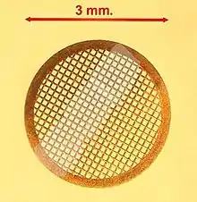
TEM specimen stage designs include airlocks to allow for insertion of the specimen holder into the vacuum with minimal loss of vacuum in other areas of the microscope. The specimen holders hold a standard size of sample grid or self-supporting specimen. Standard TEM grid sizes are 3.05 mm diameter, with a thickness and mesh size ranging from a few to 100 μm. The sample is placed onto the meshed area having a diameter of approximately 2.5 mm. Usual grid materials are copper, molybdenum, gold or platinum. This grid is placed into the sample holder, which is paired with the specimen stage. A wide variety of designs of stages and holders exist, depending upon the type of experiment being performed. In addition to 3.05 mm grids, 2.3 mm grids are sometimes, if rarely, used. These grids were particularly used in the mineral sciences where a large degree of tilt can be required and where specimen material may be extremely rare. Electron transparent specimens have a thickness usually less than 100 nm, but this value depends on the accelerating voltage.
Once inserted into a TEM, the sample has to be manipulated to locate the region of interest to the beam, such as in single grain diffraction, in a specific orientation. To accommodate this, the TEM stage allows movement of the sample in the XY plane, Z height adjustment, and commonly a single tilt direction parallel to the axis of side entry holders. Sample rotation may be available on specialized diffraction holders and stages. Some modern TEMs provide the ability for two orthogonal tilt angles of movement with specialized holder designs called double-tilt sample holders. Some stage designs, such as top-entry or vertical insertion stages once common for high resolution TEM studies, may simply only have X-Y translation available. The design criteria of TEM stages are complex, owing to the simultaneous requirements of mechanical and electron-optical constraints and specialized models are available for different methods.
A TEM stage is required to have the ability to hold a specimen and be manipulated to bring the region of interest into the path of the electron beam. As the TEM can operate over a wide range of magnifications, the stage must simultaneously be highly resistant to mechanical drift, with drift requirements as low as a few nm/minute while being able to move several μm/minute, with repositioning accuracy on the order of nanometers.[36] Earlier designs of TEM accomplished this with a complex set of mechanical downgearing devices, allowing the operator to finely control the motion of the stage by several rotating rods. Modern devices may use electrical stage designs, using screw gearing in concert with stepper motors, providing the operator with a computer-based stage input, such as a joystick or trackball.
Two main designs for stages in a TEM exist, the side-entry and top entry version.[25] Each design must accommodate the matching holder to allow for specimen insertion without either damaging delicate TEM optics or allowing gas into TEM systems under vacuum.

The most common is the side entry holder, where the specimen is placed near the tip of a long metal (brass or stainless steel) rod, with the specimen placed flat in a small bore. Along the rod are several polymer vacuum rings to allow for the formation of a vacuum seal of sufficient quality, when inserted into the stage. The stage is thus designed to accommodate the rod, placing the sample either in between or near the objective lens, dependent upon the objective design. When inserted into the stage, the side entry holder has its tip contained within the TEM vacuum, and the base is presented to atmosphere, the airlock formed by the vacuum rings.
Insertion procedures for side-entry TEM holders typically involve the rotation of the sample to trigger micro switches that initiate evacuation of the airlock before the sample is inserted into the TEM column.
The second design is the top-entry holder consists of a cartridge that is several cm long with a bore drilled down the cartridge axis. The specimen is loaded into the bore, possibly using a small screw ring to hold the sample in place. This cartridge is inserted into an airlock with the bore perpendicular to the TEM optic axis. When sealed, the airlock is manipulated to push the cartridge such that the cartridge falls into place, where the bore hole becomes aligned with the beam axis, such that the beam travels down the cartridge bore and into the specimen. Such designs are typically unable to be tilted without blocking the beam path or interfering with the objective lens.[25]
Electron gun

The electron gun is formed from several components: the filament, a biasing circuit, a Wehnelt cap, and an extraction anode. By connecting the filament to the negative component power supply, electrons can be "pumped" from the electron gun to the anode plate and the TEM column, thus completing the circuit. The gun is designed to create a beam of electrons exiting from the assembly at some given angle, known as the gun divergence semi-angle, α. By constructing the Wehnelt cylinder such that it has a higher negative charge than the filament itself, electrons that exit the filament in a diverging manner are, under proper operation, forced into a converging pattern the minimum size of which is the gun crossover diameter.
The thermionic emission current density, J, can be related to the work function of the emitting material via Richardson's law
where A is the Richardson's constant, Φ is the work function and T is the temperature of the material.[25]
This equation shows that in order to achieve sufficient current density it is necessary to heat the emitter, taking care not to cause damage by application of excessive heat. For this reason materials with either a high melting point, such as tungsten, or those with a low work function (LaB6) are required for the gun filament.[37] Furthermore, both lanthanum hexaboride and tungsten thermionic sources must be heated in order to achieve thermionic emission, this can be achieved by the use of a small resistive strip. To prevent thermal shock, there is often a delay enforced in the application of current to the tip, to prevent thermal gradients from damaging the filament, the delay is usually a few seconds for LaB6, and significantly lower for tungsten.
Electron lens

Electron lenses are designed to act in a manner emulating that of an optical lens, by focusing parallel electrons at some constant focal distance. Electron lenses may operate electrostatically or magnetically. The majority of electron lenses for TEM use electromagnetic coils to generate a convex lens. The field produced for the lens must be radially symmetrical, as deviation from the radial symmetry of the magnetic lens causes aberrations such as astigmatism, and worsens spherical and chromatic aberration. Electron lenses are manufactured from iron, iron-cobalt or nickel cobalt alloys,[38] such as permalloy. These are selected for their magnetic properties, such as magnetic saturation, hysteresis and permeability.
The components include the yoke, the magnetic coil, the poles, the polepiece, and the external control circuitry. The pole piece must be manufactured in a very symmetrical manner, as this provides the boundary conditions for the magnetic field that forms the lens. Imperfections in the manufacture of the pole piece can induce severe distortions in the magnetic field symmetry, which induce distortions that will ultimately limit the lenses' ability to reproduce the object plane. The exact dimensions of the gap, pole piece internal diameter and taper, as well as the overall design of the lens is often performed by finite element analysis of the magnetic field, whilst considering the thermal and electrical constraints of the design.[38]
The coils which produce the magnetic field are located within the lens yoke. The coils can contain a variable current, but typically use high voltages, and therefore require significant insulation in order to prevent short-circuiting the lens components. Thermal distributors are placed to ensure the extraction of the heat generated by the energy lost to resistance of the coil windings. The windings may be water-cooled, using a chilled water supply in order to facilitate the removal of the high thermal duty.
Apertures
Apertures are annular metallic plates, through which electrons that are further than a fixed distance from the optic axis may be excluded. These consist of a small metallic disc that is sufficiently thick to prevent electrons from passing through the disc, whilst permitting axial electrons. This permission of central electrons in a TEM causes two effects simultaneously: firstly, apertures decrease the beam intensity as electrons are filtered from the beam, which may be desired in the case of beam sensitive samples. Secondly, this filtering removes electrons that are scattered to high angles, which may be due to unwanted processes such as spherical or chromatic aberration, or due to diffraction from interaction within the sample.[39]
Apertures are either a fixed aperture within the column, such as at the condenser lens, or are a movable aperture, which can be inserted or withdrawn from the beam path, or moved in the plane perpendicular to the beam path. Aperture assemblies are mechanical devices which allow for the selection of different aperture sizes, which may be used by the operator to trade off intensity and the filtering effect of the aperture. Aperture assemblies are often equipped with micrometers to move the aperture, required during optical calibration.
Imaging methods
Imaging methods in TEM use the information contained in the electron waves exiting from the sample to form an image. The projector lenses allow for the correct positioning of this electron wave distribution onto the viewing system. The observed intensity, I, of the image, assuming sufficiently high quality of imaging device, can be approximated as proportional to the time-averaged squared absolute value of the amplitude of the electron wavefunctions, where the wave that forms the exit beam is denoted by Ψ.[40]
Different imaging methods therefore attempt to modify the electron waves exiting the sample in a way that provides information about the sample, or the beam itself. From the previous equation, it can be deduced that the observed image depends not only on the amplitude of beam, but also on the phase of the electrons, although phase effects may often be ignored at lower magnifications. Higher resolution imaging requires thinner samples and higher energies of incident electrons, which means that the sample can no longer be considered to be absorbing electrons (i.e., via a Beer's law effect). Instead, the sample can be modeled as an object that does not change the amplitude of the incoming electron wave function, but instead modifies the phase of the incoming wave; in this model, the sample is known as a pure phase object. For sufficiently thin specimens, phase effects dominate the image, complicating analysis of the observed intensities.[40] To improve the contrast in the image, the TEM may be operated at a slight defocus to enhance contrast, owing to convolution by the contrast transfer function of the TEM,[41] which would normally decrease contrast if the sample was not a weak phase object.
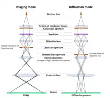
The figure on the right shows the two basic operation modes of TEM – imaging and diffraction modes. In both cases the specimen is illuminated with the parallel beam, formed by electron beam shaping with the system of Condenser lenses and Condenser aperture. After interaction with the sample, on the exit surface of the specimen two types of electrons exist – unscattered (which will correspond to the bright central beam on the diffraction pattern) and scattered electrons (which change their trajectories due to interaction with the material).
In Imaging mode, the objective aperture is inserted in a back focal plane (BFP) of the objective lens (where diffraction spots are formed). If using the objective aperture to select only the central beam, the transmitted electrons are passed through the aperture while all others are blocked, and a bright field image (BF image) is obtained. If we allow the signal from a diffracted beam, a dark field image (DF image) is received. The selected signal is magnified and projected on a screen (or on a camera) with the help of Intermediate and Projector lenses. An image of the sample is thus obtained.
In Diffraction mode, a selected area aperture may be used to determine more precisely the specimen area from which the signal will be displayed. By changing the strength of current to the intermediate lens, the diffraction pattern is projected on a screen. Diffraction is a very powerful tool for doing a cell reconstruction and crystal orientation determination.
Contrast formation
The contrast between two adjacent areas in a TEM image can be defined as the difference in the electron densities in image plane. Due to the scattering of the incident beam by the sample, the amplitude and phase of the electron wave change, which results in amplitude contrast and phase contrast, correspondingly. Most images have both contrast components.
Amplitude–contrast is obtained due to removal of some electrons before the image plane. During their interaction with the specimen some of electrons will be lost due to absorption, or due to scattering at very high angles beyond the physical limitation of microscope or are blocked by the objective aperture. While the first two losses are due to the specimen and microscope construction, the objective aperture can be used by operator to enhance the contrast.

Figure on the right shows a TEM image (a) and the corresponding diffraction pattern (b) of Pt polycrystalline film taken without an objective aperture. In order to enhance the contrast in the TEM image the number of scattered beams as visible in the diffraction pattern should be reduced. This can be done by selecting a certain area in the back focal plane such as only the central beam or a specific diffracted beam (angle), or combinations of such beams. By intentionally selecting an objective aperture which only permits the non-diffracted beam to pass beyond the back focal plane (and onto the image plane): one creates a Bright-Field (BF) image (c), whereas if the central, non-diffracted beam is blocked: one may obtain Dark-Field (DF) images such as those shown in (d-e). The DF images (d-e) were obtained by selecting the diffracted beams indicated in diffraction pattern with circles (b) using an aperture at the back focal plane. Grains from which electrons are scattered into these diffraction spots appear brighter. More details about diffraction contrast formation are given further.
There are two types of amplitude contrast – mass–thickness and diffraction contrast. First, let's consider mass–thickness contrast. When the beam illuminates two neighbouring areas with low mass (or thickness) and high mass (or thickness), the heavier region scatters electrons at bigger angles. These strongly scattered electrons are blocked in BF TEM mode by objective aperture. As a result, heavier regions appear darker in BF images (have low intensity). Mass–thickness contrast is most important for non–crystalline, amorphous materials.
Diffraction contrast occurs due to a specific crystallographic orientation of a grain. In such a case the crystal is oriented in a way that there is a high probability of diffraction. Diffraction contrast provides information on the orientation of the crystals in a polycrystalline sample, as well as other information such as defects. Note that in case diffraction contrast exists, the contrast cannot be interpreted as due to mass or thickness variations.
Diffraction contrast

Samples can exhibit diffraction contrast, whereby the electron beam undergoes diffraction which in the case of a crystalline sample, disperses electrons into discrete locations in the back focal plane. By the placement of apertures in the back focal plane, i.e. the objective aperture, the desired reciprocal lattice vectors can be selected (or excluded), thus only parts of the sample that are causing the electrons to scatter to the selected reflections will end up projected onto the imaging apparatus.
If the reflections that are selected do not include the unscattered beam (which will appear up at the focal point of the lens), then the image will appear dark wherever no sample scattering to the selected peak is present, as such a region without a specimen will appear dark. This is known as a dark-field image.
Modern TEMs are often equipped with specimen holders that allow the user to tilt the specimen to a range of angles in order to obtain specific diffraction conditions, and apertures placed above the specimen allow the user to select electrons that would otherwise be diffracted in a particular direction from entering the specimen.
Applications for this method include the identification of lattice defects in crystals. By carefully selecting the orientation of the sample, it is possible not just to determine the position of defects but also to determine the type of defect present. If the sample is oriented so that one particular plane is only slightly tilted away from the strongest diffracting angle (known as the Bragg Angle), any distortion of the crystal plane that locally tilts the plane to the Bragg angle will produce particularly strong contrast variations. However, defects that produce only displacement of atoms that do not tilt the crystal towards the Bragg angle (i. e. displacements parallel to the crystal plane) will produce weaker contrast.[42]
Phase contrast
Crystal structure can also be investigated by high-resolution transmission electron microscopy (HRTEM), also known as phase contrast. When using a field emission source and a specimen of uniform thickness, the images are formed due to differences in phase of electron waves, which is caused by specimen interaction.[41] Image formation is given by the complex modulus of the incoming electron beams. As such, the image is not only dependent on the number of electrons hitting the screen, making direct interpretation of phase contrast images slightly more complex. However this effect can be used to an advantage, as it can be manipulated to provide more information about the sample, such as in complex phase retrieval techniques.
Diffraction
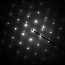
As previously stated, by adjusting the magnetic lenses such that the back focal plane of the lens rather than the imaging plane is placed on the imaging apparatus a diffraction pattern can be generated. For thin crystalline samples, this produces an image that consists of a pattern of dots in the case of a single crystal, or a series of rings in the case of a polycrystalline or amorphous solid material. For the single crystal case the diffraction pattern is dependent upon the orientation of the specimen and the structure of the sample illuminated by the electron beam. This image provides the investigator with information about the space group symmetries in the crystal and the crystal's orientation to the beam path. This is typically done without using any information but the position at which the diffraction spots appear and the observed image symmetries.
Diffraction patterns can have a large dynamic range, and for crystalline samples, may have intensities greater than those recordable by CCD. As such, TEMs may still be equipped with film cartridges for the purpose of obtaining these images, as the film is a single use detector.
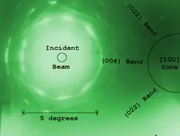
Analysis of diffraction patterns beyond point-position can be complex, as the image is sensitive to a number of factors such as specimen thickness and orientation, objective lens defocus, and spherical and chromatic aberration. Although quantitative interpretation of the contrast shown in lattice images is possible, it is inherently complicated and can require extensive computer simulation and analysis, such as electron multislice analysis.[43]
More complex behavior in the diffraction plane is also possible, with phenomena such as Kikuchi lines arising from multiple diffraction within the crystalline lattice. In convergent beam electron diffraction (CBED) where a non-parallel, i.e. converging, electron wavefront is produced by concentrating the electron beam into a fine probe at the sample surface, the interaction of the convergent beam can provide information beyond structural data such as sample thickness.
Electron energy loss spectroscopy (EELS)
Using the advanced technique of electron energy loss spectroscopy (EELS), for TEMs appropriately equipped, electrons can be separated into a spectrum based upon their velocity (which is closely related to their kinetic energy, and thus energy loss from the beam energy), using magnetic sector based devices known as EEL spectrometers. These devices allow for the selection of particular energy values, which can be associated with the way the electron has interacted with the sample. For example, different elements in a sample result in different electron energies in the beam after the sample. This normally results in chromatic aberration – however this effect can, for example, be used to generate an image which provides information on elemental composition, based upon the atomic transition during electron-electron interaction.[44]
EELS spectrometers can often be operated in both spectroscopic and imaging modes, allowing for isolation or rejection of elastically scattered beams. As for many images inelastic scattering will include information that may not be of interest to the investigator thus reducing observable signals of interest, EELS imaging can be used to enhance contrast in observed images, including both bright field and diffraction, by rejecting unwanted components.
Three-dimensional imaging
As TEM specimen holders typically allow for the rotation of a sample by a desired angle, multiple views of the same specimen can be obtained by rotating the angle of the sample along an axis perpendicular to the beam. By taking multiple images of a single TEM sample at differing angles, typically in 1° increments, a set of images known as a "tilt series" can be collected. This methodology was proposed in the 1970s by Walter Hoppe. Under purely absorption contrast conditions, this set of images can be used to construct a three-dimensional representation of the sample.[46]
The reconstruction is accomplished by a two-step process, first images are aligned to account for errors in the positioning of a sample; such errors can occur due to vibration or mechanical drift.[47] Alignment methods use image registration algorithms, such as autocorrelation methods to correct these errors. Secondly, using a reconstruction algorithm, such as filtered back projection, the aligned image slices can be transformed from a set of two-dimensional images, Ij(x, y), to a single three-dimensional image, I'j(x, y, z). This three-dimensional image is of particular interest when morphological information is required, further study can be undertaken using computer algorithms, such as isosurfaces and data slicing to analyse the data.
As TEM samples cannot typically be viewed at a full 180° rotation, the observed images typically suffer from a "missing wedge" of data, which when using Fourier-based back projection methods decreases the range of resolvable frequencies in the three-dimensional reconstruction.[46] Mechanical refinements, such as multi-axis tilting (two tilt series of the same specimen made at orthogonal directions) and conical tomography (where the specimen is first tilted to a given fixed angle and then imaged at equal angular rotational increments through one complete rotation in the plane of the specimen grid) can be used to limit the impact of the missing data on the observed specimen morphology. Using focused ion beam milling, a new technique has been proposed[48] which uses pillar-shaped specimen and a dedicated on-axis tomography holder to perform 180° rotation of the sample inside the pole piece of the objective lens in TEM. Using such arrangements, quantitative electron tomography without the missing wedge is possible.[49] In addition, numerical techniques exist which can improve the collected data.
All the above-mentioned methods involve recording tilt series of a given specimen field. This inevitably results in the summation of a high dose of reactive electrons through the sample and the accompanying destruction of fine detail during recording. The technique of low-dose (minimal-dose) imaging is therefore regularly applied to mitigate this effect. Low-dose imaging is performed by deflecting illumination and imaging regions simultaneously away from the optical axis to image an adjacent region to the area to be recorded (the high-dose region). This area is maintained centered during tilting and refocused before recording. During recording the deflections are removed so that the area of interest is exposed to the electron beam only for the duration required for imaging. An improvement of this technique (for objects resting on a sloping substrate film) is to have two symmetrical off-axis regions for focusing followed by setting focus to the average of the two high-dose focus values before recording the low-dose area of interest.
Non-tomographic variants on this method, referred to as single particle analysis, use images of multiple (hopefully) identical objects at different orientations to produce the image data required for three-dimensional reconstruction. If the objects do not have significant preferred orientations, this method does not suffer from the missing data wedge (or cone) which accompany tomographic methods nor does it incur excessive radiation dosage, however it assumes that the different objects imaged can be treated as if the 3D data generated from them arose from a single stable object.
Sample preparation
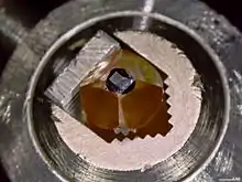
Sample preparation in TEM can be a complex procedure.[50] TEM specimens should be less than 100 nanometers thick for a conventional TEM. Unlike neutron or X-ray radiation the electrons in the beam interact readily with the sample, an effect that increases roughly with atomic number squared (Z2).[15] High quality samples will have a thickness that is comparable to the mean free path of the electrons that travel through the samples, which may be only a few tens of nanometers. Preparation of TEM specimens is specific to the material under analysis and the type of information to be obtained from the specimen.
Materials that have dimensions small enough to be electron transparent, such as powdered substances, small organisms, viruses, or nanotubes, can be quickly prepared by the deposition of a dilute sample containing the specimen onto films on support grids. Biological specimens may be embedded in resin to withstand the high vacuum in the sample chamber and to enable cutting tissue into electron transparent thin sections. The biological sample can be stained using either a negative staining material such as uranyl acetate for bacteria and viruses, or, in the case of embedded sections, the specimen may be stained with heavy metals, including osmium tetroxide. Alternately samples may be held at liquid nitrogen temperatures after embedding in vitreous ice.[51] In material science and metallurgy the specimens can usually withstand the high vacuum, but still must be prepared as a thin foil, or etched so some portion of the specimen is thin enough for the beam to penetrate. Constraints on the thickness of the material may be limited by the scattering cross-section of the atoms from which the material is comprised.
Tissue sectioning
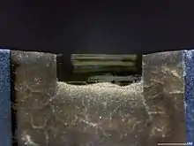
Biological tissue is often embedded in a resin block then thinned to less than 100 nm on an ultramicrotome. The resin block is fractured as it passes over a glass or diamond knife edge.[52] This method is used to obtain thin, minimally deformed samples that allow for the observation of tissue ultrastructure. Inorganic samples, such as aluminium, may also be embedded in resins and ultrathin sectioned in this way, using either coated glass, sapphire or larger angle diamond knives.[53] To prevent charge build-up at the sample surface when viewing in the TEM, tissue samples need to be coated with a thin layer of conducting material, such as carbon.
Sample staining
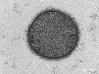
TEM samples of biological tissues need high atomic number stains to enhance contrast. The stain absorbs the beam electrons or scatters part of the electron beam which otherwise is projected onto the imaging system. Compounds of heavy metals such as osmium, lead, uranium or gold (in immunogold labelling) may be used prior to TEM observation to selectively deposit electron dense atoms in or on the sample in desired cellular or protein region. This process requires an understanding of how heavy metals bind to specific biological tissues and cellular structures.[54]
Mechanical milling
Mechanical polishing is also used to prepare samples for imaging on the TEM. Polishing needs to be done to a high quality, to ensure constant sample thickness across the region of interest. A diamond, or cubic boron nitride polishing compound may be used in the final stages of polishing to remove any scratches that may cause contrast fluctuations due to varying sample thickness. Even after careful mechanical milling, additional fine methods such as ion etching may be required to perform final stage thinning.
Chemical etching
Certain samples may be prepared by chemical etching, particularly metallic specimens. These samples are thinned using a chemical etchant, such as an acid, to prepare the sample for TEM observation. Devices to control the thinning process may allow the operator to control either the voltage or current passing through the specimen, and may include systems to detect when the sample has been thinned to a sufficient level of optical transparency.
Ion etching
Ion etching is a sputtering process that can remove very fine quantities of material. This is used to perform a finishing polish of specimens polished by other means. Ion etching uses an inert gas passed through an electric field to generate a plasma stream that is directed to the sample surface. Acceleration energies for gases such as argon are typically a few kilovolts. The sample may be rotated to promote even polishing of the sample surface. The sputtering rate of such methods is on the order of tens of micrometers per hour, limiting the method to only extremely fine polishing.
Ion etching by argon gas has been recently shown to be able to file down MTJ stack structures to a specific layer which has then been atomically resolved. The TEM images taken in plan view rather than cross-section reveal that the MgO layer within MTJs contains a large number of grain boundaries that may be diminishing the properties of devices.[55]
Ion milling (FIB)

More recently focused ion beam methods have been used to prepare samples. FIB is a relatively new technique to prepare thin samples for TEM examination from larger specimens. Because FIB can be used to micro-machine samples very precisely, it is possible to mill very thin membranes from a specific area of interest in a sample, such as a semiconductor or metal. Unlike inert gas ion sputtering, FIB makes use of significantly more energetic gallium ions and may alter the composition or structure of the material through gallium implantation.[56]
Nanowire assisted transfer
For a minimal introduction of stress and bending to transmission electron microscopy (TEM) samples (lamellae, thin films, and other mechanically and beam sensitive samples), when transferring inside a focused ion beam (FIB), flexible metallic nanowires can be attached to a typically rigid micromanipulator.
The main advantages of this method include a significant reduction of sample preparation time (quick welding and cutting of nanowire at low beam current), and minimization of stress-induced bending, Pt contamination, and ion beam damage.[57] This technique is particularly suitable for in situ electron microscopy sample preparation.
Replication
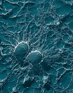
Samples may also be replicated using cellulose acetate film, the film subsequently coated with a heavy metal such as platinum, the original film dissolved away, and the replica imaged on the TEM. Variations of the replica technique are used for both materials and biological samples. In materials science a common use is for examining the fresh fracture surface of metal alloys.
Modifications
The capabilities of the TEM can be further extended by additional stages and detectors, sometimes incorporated on the same microscope.
Scanning TEM
A TEM can be modified into a scanning transmission electron microscope (STEM) by the addition of a system that rasters a convergent beam across the sample to form the image, when combined with suitable detectors. Scanning coils are used to deflect the beam, such as by an electrostatic shift of the beam, where the beam is then collected using a current detector such as a Faraday cup, which acts as a direct electron counter. By correlating the electron count to the position of the scanning beam (known as the "probe"), the transmitted component of the beam may be measured. The non-transmitted components may be obtained either by beam tilting or by the use of annular dark field detectors.
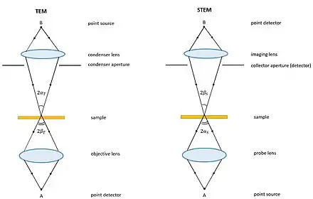
Fundamentally, TEM and STEM are linked via Helmholtz reciprocity. A STEM is a TEM in which the electron source and observation point have been switched relative to the direction of travel of the electron beam. See the ray diagrams in the figure on the right. The STEM instrument effectively relies on the same optical set-up as a TEM, but operates by flipping the direction of travel of the electrons (or reversing time) during operation of a TEM. Rather than using an aperture to control detected electrons, as in TEM, a STEM uses various detectors with collection angles that may be adjusted depending on which electrons the user wants to capture.
Low-voltage electron microscope
A low-voltage electron microscope (LVEM) is operated at relatively low electron accelerating voltage between 5–25 kV. Some of these can be a combination of SEM, TEM and STEM in a single compact instrument. Low voltage increases image contrast which is especially important for biological specimens. This increase in contrast significantly reduces, or even eliminates the need to stain. Resolutions of a few nm are possible in TEM, SEM and STEM modes. The low energy of the electron beam means that permanent magnets can be used as lenses and thus a miniature column that does not require cooling can be used.[58][59]
Cryo-TEM
Cryogenic transmission electron microscopy (Cryo-TEM) uses a TEM with a specimen holder capable of maintaining the specimen at liquid nitrogen or liquid helium temperatures. This allows imaging specimens prepared in vitreous ice, the preferred preparation technique for imaging individual molecules or macromolecular assemblies,[60] imaging of vitrified solid-electrolye interfaces,[61] and imaging of materials that are volatile in high vacuum at room temperature, such as sulfur.[62]
Environmental/In-situ TEM
In-situ experiments may also be conducted in TEM using differentially pumped sample chambers, or specialized holders.[63] Types of in-situ experiments include studying nanomaterials,[64] biological specimens, chemical reactions of molecules,[65] liquid-phase electron microscopy,[66][67] and material deformation testing.[68]
High Temperature In-Situ TEM
Many phase transformations occur during heating. Additionally, coarsening and grain growth, along with other diffusion-related processes occur more rapidly at elevated temperatures, where kinetics are improved, allowing for the observation of related phenomena under transmission electron microscopy within reasonable time scales. This also allows for the observation of phenomena that occur at elevated temperatures and disappear or are not uniformly preserved in ex-situ samples.
High temperature TEM introduces various additional challenges which must be addressed in the mechanics of high temperature holders, including but not limited to drift-correction, temperature measurement, and decreased spatial resolution at the expense of more complex holders.[69][70]
Sample drift in the TEM is linearly proportional to the temperature differential between the room and holder. With temperatures as high as 1500C in modern holders, samples may experience significant drift and vertical displacement (bulging), requiring continuous focus or stage adjustments, inducing resolution loss and mechanical drift.[71][72] Individual labs and manufacturers have developed software coupled with advanced cooling systems to correct for thermal drift based on the predicted temperature in the sample chamber[69][72][73] These systems often take 30 min-many hours for sample shifts to stabilize. While significant progress has been made, no universal TEM attachment has been made to account for drift at elevated temperatures.[70][71][73]
An additional challenge of many of these specialized holders is knowing the local sample temperature. Many high temperature holders utilize a tungsten filament to locally heat the sample.[69][72] Ambiguity in temperature in furnace heaters (W wire) with thermocouples arises from the thermal contact between the furnace and the TEM grid; complicated by temperature gradients along the sample caused by varying thermal conductivity with different samples and grid materials.[70] With different holders both commercial and lab made, different methods for creating temperature calibration are available. Manufacturers like Gatan use IR pyrometry to measure temperature gradients over their entire sample. An even better method to calibrate is Raman spectroscopy which measures the local temperature of Si powder on electron transparent windows and quantitatively calibrates the IR pyrometry. These measurements have guaranteed accuracy within 5%. Research laboratories have also performed their own calibrations on commercial holders. Researchers at NIST utilized Raman spectroscopy to map the temperature profile of a sample on a TEM grid and achieve very precise measurements to enhance their research.[74] Similarly, a research group in Germany utilized X-ray diffraction to measure slight shifts in lattice spacing caused by changes in temperature to back calculate the exact temperature in the holder. This process required careful calibration and exact TEM optics.[75] Other examples include the use of EELS to measure local temperature using change of gas density,[76] and resistivity changes.[70]
Optimal resolution in a TEM is achieved when spherical aberrations are corrected with objective lens. However, due to the geometry of most TEMs, inserting large in-situ holders requires the user to compromise the objective lens and endure spherical aberrations. Therefore, there is a compromise between the width of the pole-piece gap and spatial resolution below 0.1 nm. Research groups at various institutions have tried to overcome spherical aberrations through use of monochromators to achieve 0.05 nm resolution with a 5 mm pole piece gap.[77]
In-Situ Mechanical TEM
High resolution of TEM allows for monitoring the sample in question on a length scale ranging from hundreds of nanometers to several angstroms. This allows for the visualization of both elastic and plastic deformation via strain fields as well as the motion of crystallographic defects such as lattice distortions and dislocation motion. By simultaneously observing deformation phenomena and measuring mechanical response in situ, it is possible to connect nano-mechanical testing information to models that describe both the subtlety and complexity of how materials respond to stress and strain.[78] The material properties and data accuracy obtained from such nano-mechanical tests is largely determined by the mechanical straining holder being used. Current straining holders have the ability to perform tensile tests, nano-indentation, compression tests, shear tests and bending tests on materials.[79]
Classical Mechanical Holders
One of the pioneers of classical holders was Heinz G.F. Wilsdorf, who conducted a tensile test inside a TEM in 1958.[80] In a typical experiment, electron transparent TEM samples are cut to shape and glued to a deformable grid. Advances in micromanipulators have also enabled the tensile testing of nanowires and thin films. The deformable grid attaches to the classical tensile holder which stretches the sample using a long rigid shaft attached to a worm gear box actuated by an electric motor located in a housing outside the TEM. Typically strain rates range from 10 nm/s to 10 μm/s.[81] Custom-made holders expanding simple straining actuation have enabled bending tests using a bending holder[82] and shear tests using a shear sample holder.[83] The typical measured sample properties in these experiments are yield strength, elastic modulus, shear modulus, tensile strength, bending strength, and shear strength. In order to study the temperature-dependent mechanical properties of TEM samples, the holder can be cooled through a cold finger connected to a liquid nitrogen reservoir. For high temperature experiments, the TEM sample can also be heated through a miniaturized furnace or a laser that can typically reach 1000 °C.[84]
Nano-Indentation Holders
Nano-Indentation holders perform a hardness test on the material in question by pressing a hard tip into a polished flat surface and measuring the applied force and the resulting displacement on the TEM sample through a change in capacitance between a reference and a movable electrostatic plate attached to the tip.[85] The typical measured sample properties are hardness and elastic modulus. Although nano-indentation was possible since early 1980s, its investigation using a TEM was first reported in 2001 where an aluminum sample deposited on a silicon wedge was investigated.[86] For nanoindentation experiments, TEM samples are typically shaped as wedges using a tripod polisher, H-bar window or a micro-nanopillar using focused ion beam to create enough space for a tip to be pressed at the desired electron transparent location. The indenter tips are typically flat punch-type, pyramidal, or wedge shaped elongated in the z-direction.[87] Pyramidal tips offer high precision on the order of 10 nm but suffer from sample slip, while wedge indenters have greater contract to prevent slipping but require finite element analysis to model the transmitted stress since the high contact area with the TEM sample makes this almost a compression test.[88]
Micro Electro-Mechanical Systems (MEMs)
Micro Electro-Mechanical Systems (MEMs) based holders provide a cheap and customizable platform to conduct mechanical tests on previously difficult samples to work with such as micropillars, nanowires, and thin films.[89] Passive MEMs are used as simple push to pull devices for in-situ mechanical tests. Typically, a nano-indentation holder is used to apply a pushing force at the indentation site. Using a geometry of arms, this pushing force translates to a pulling force on a pair of tensile pads to which the sample is attached. Thus, a compression applied on the outside of the MEMs translates to a tension in the central gap where the TEM sample is located. The resulting force-displacement curve needs to be corrected by performing the same test on an empty MEMs without the TEM sample to account for the stiffness of the empty MEMs. The dimensions and stiffness of the MEMs can be modified to perform tensile tests on different sized samples with different loads. To smoothen the actuation process, active MEMs have been developed with built-in actuators and sensors. These devices work by applying a stress using electrical power and measuring strain using capacitance variations.[90] Electrostatically actuated MEMs have also been developed to accommodate very low applied forces in the 1-100 nN range.[91]
Much of current research focuses on developing sample holders that can perform mechanical tests while creating an environmental stimulus such as temperature change, variable strain rates, and different gas environments. In addition, the emergence of high resolution detectors are allowing to monitor dislocation motion and interactions with other defects and pushing the limits of sub-nanometer strain measurements. In Situ Mechanical TEM measurements are routinely coupled with other standard TEM measurements such as EELS and XEDS to reach a comprehensive understanding of the sample structure and properties.[92]
Aberration corrected TEM
Modern research TEMs may include aberration correctors,[19] to reduce the amount of distortion in the image. Incident beam monochromators may also be used which reduce the energy spread of the incident electron beam to less than 0.15 eV.[19] Major aberration corrected TEM manufacturers include JEOL, Hitachi High-technologies, FEI Company, and NION.
Ultrafast and dynamic TEM
It is possible to reach temporal resolution far beyond that of the readout rate of electron detectors with the use of pulsed electrons. Pulses can be produced by either modifying the electron source to enable laser-triggered photoemission[93] or by installation of an ultrafast beam blanker.[94] This approach is termed ultrafast transmission electron microscopy when stroboscopic pump-probe illumination is used: an image is formed by the accumulation of many ultrashort electron pulses (typically of hundreds of femtoseconds) with a fixed time delay between the arrival of the electron pulse and the sample excitation. On the other hand, the use of single or a short sequence of electron pulses with a sufficient number of electrons to form an image from each pulse is called dynamic transmission electron microscopy. Temporal resolution down to hundreds of femtoseconds and spatial resolution comparable to that available with a Schottky field emission source is possible in ultrafast TEM,[95] but the technique can only image reversible processes that can be reproducibly triggered millions of times. Dynamic TEM can resolve irreversible processes down to tens of nanoseconds and tens of nanometers.[96]
The technique has been pioneered at the early 2000s in laboratories in Germany (Technical University Berlin[93]) and in the USA (Caltech[97][98] and Lawrence Livermore National Laboratory[99] [100] ). Ultrafast TEM and Dynamic TEM have made possible real-time investigation of numerous physical and chemical phenomena at the nanoscale.
An interesting variant of the Ultrafast Transmission Electron Microscopy technique is the Photon-Induced Near-field Electron Microscopy (PINEM). The latter is based on the inelastic coupling between electrons and photons in presence of a surface or a nanostructure.[101] This method allows one to investigate time-varying nanoscale electromagnetic fields in an electron microscope, as well as dynamically shape the wave properties of the electron beam.
Limitations
There are a number of drawbacks to the TEM technique. Many materials require extensive sample preparation to produce a sample thin enough to be electron transparent, which makes TEM analysis a relatively time-consuming process with a low throughput of samples. The structure of the sample may also be changed during the preparation process. Also the field of view is relatively small, raising the possibility that the region analyzed may not be characteristic of the whole sample. There is potential that the sample may be damaged by the electron beam, particularly in the case of biological materials.
Resolution limits
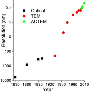
The limit of resolution obtainable in a TEM may be described in several ways, and is typically referred to as the information limit of the microscope. One commonly used value is a cut-off value of the contrast transfer function, a function that is usually quoted in the frequency domain to define the reproduction of spatial frequencies of objects in the object plane by the microscope optics. A cut-off frequency, qmax, for the transfer function may be approximated with the following equation, where Cs is the spherical aberration coefficient and λ is the electron wavelength:[39]
For a 200 kV microscope, with partly corrected spherical aberrations ("to the third order") and a Cs value of 1 µm,[103] a theoretical cut-off value might be 1/qmax = 42 pm.[39] The same microscope without a corrector would have Cs = 0.5 mm and thus a 200-pm cut-off.[103] The spherical aberrations are suppressed to the third or fifth order in the "aberration-corrected" microscopes. Their resolution is however limited by electron source geometry and brightness and chromatic aberrations in the objective lens system.[19][104]
The frequency domain representation of the contrast transfer function may often have an oscillatory nature,[105] which can be tuned by adjusting the focal value of the objective lens. This oscillatory nature implies that some spatial frequencies are faithfully imaged by the microscope, whilst others are suppressed. By combining multiple images with different spatial frequencies, the use of techniques such as focal series reconstruction can be used to improve the resolution of the TEM in a limited manner.[39] The contrast transfer function can, to some extent, be experimentally approximated through techniques such as Fourier transforming images of amorphous material, such as amorphous carbon.
More recently, advances in aberration corrector design have been able to reduce spherical aberrations[106] and to achieve resolution below 0.5 Ångströms (50 pm)[104] at magnifications above 50 million times.[107] Improved resolution allows for the imaging of lighter atoms that scatter electrons less efficiently, such as lithium atoms in lithium battery materials.[108] The ability to determine the position of atoms within materials has made the HRTEM an indispensable tool for nanotechnology research and development in many fields, including heterogeneous catalysis and the development of semiconductor devices for electronics and photonics.[109]
See also
- Electron microscope
- Cryo-electron microscopy
- Electron diffraction
- Electron energy loss spectroscopy (EELS)
- Energy filtered transmission electron microscopy (EFTEM)
- High-resolution transmission electron microscopy (HRTEM)
- Low-voltage electron microscope (LVEM)
- Precession electron diffraction
- Scanning confocal electron microscopy
References
- "Viruses". users.rcn.com.
- "The Nobel Prize in Physics 1986, Perspectives – Life through a Lens". nobelprize.org.
- ultraviolet microscope. (2010). In Encyclopædia Britannica. Retrieved November 20, 2010, from Encyclopædia Britannica Online
- Ernst Ruska (January 1980). The Early Development of Electron Lenses and Electron Microscopy. Applied Optics. Vol. 25. Translated by T. Mulvey. p. 820. Bibcode:1986ApOpt..25..820R. ISBN 978-3-7776-0364-3.
- Plücker, J. (1858). "Über die Einwirkung des Magneten auf die elektrischen Entladungen in verdünnten Gasen" [On the effect of a magnet on the electric discharge in rarified gases]. Poggendorffs Annalen der Physik und Chemie. 103 (1): 88–106. Bibcode:1858AnP...179...88P. doi:10.1002/andp.18581790106.
- "Ferdinand Braun, The Nobel Prize in Physics 1909, Biography". nobelprize.org.
- Rudenberg, Reinhold (May 30, 1931). "Configuration for the enlarged imaging of objects by electron beams". Patent DE906737.
- de Broglie, Louis Victor. "On the Theory of Quanta" (PDF). Foundation of Louis de Broglie (English translation by A.F. Kracklauer, 2004. ed.). Retrieved 25 February 2023.
- "A Brief History of the Microscopy Society of America". microscopy.org.
- "Dr. James Hillier, Biography". comdir.bfree.on.ca. Archived from the original on 2008-06-19. Retrieved 2008-09-09.
- Hawkes, P., ed. (1985). The beginnings of Electron Microscopy. Academic Press. ISBN 978-0120145782.
- "Ernst Ruska, Nobel Prize Lecture". nobelprize.org.
- Crewe, Albert V; Isaacson, M.; Johnson, D. (1969). "A Simple Scanning Electron Microscope". Rev. Sci. Instrum. 40 (2): 241–246. Bibcode:1969RScI...40..241C. doi:10.1063/1.1683910.
- Crewe, Albert V.; Wall, J.; Langmore, J. (1970). "Visibility of a single atom". Science. 168 (3937): 1338–1340. Bibcode:1970Sci...168.1338C. doi:10.1126/science.168.3937.1338. PMID 17731040. S2CID 31952480.
- Fultz, B & Howe, J (2007). Transmission Electron Microscopy and Diffractometry of Materials. Springer. ISBN 978-3-540-73885-5.
- Murphy, Douglas B. (2002). Fundamentals of Light Microscopy and Electronic Imaging. New York: John Wiley & Sons. ISBN 978-0-471-23429-6.
- Champness, P. E. (2001). Electron Diffraction in the Transmission Electron Microscope. Garland Science. ISBN 978-1-85996-147-6.
- Egerton, R (2005). Physical principles of electron microscopy. Springer. ISBN 978-0-387-25800-3.
- Rose, H H (2008). "Optics of high-performance electron Microscopes". Science and Technology of Advanced Materials. 9 (1): 014107. Bibcode:2008STAdM...9a4107R. doi:10.1088/0031-8949/9/1/014107. PMC 5099802. PMID 27877933.
- "The objective lens of a TEM, the heart of the electron microscope". rodenburg.org.
- Pogany, A. P.; Turner, P. S. (1968-01-23). "Reciprocity in electron diffraction and microscopy". Acta Crystallographica Section A. 24 (1): 103–109. Bibcode:1968AcCrA..24..103P. doi:10.1107/S0567739468000136. ISSN 1600-5724.
- Hren, John J.; Goldstein, Joseph I.; Joy, David C., eds. (1979). Introduction to Analytical Electron Microscopy. doi:10.1007/978-1-4757-5581-7. ISBN 978-1-4757-5583-1.
- Faruqi, A.R; Henderson, R. (October 2007). "Electronic detectors for electron microscopy". Current Opinion in Structural Biology. 17 (5): 549–555. doi:10.1016/j.sbi.2007.08.014. PMID 17913494.
- Henderson, R.; Cattermole, D.; McMullan, G.; Scotcher, S.; Fordham, M.; Amos, W.B.; Faruqi, A.R. (February 2007). "Digitisation of electron microscope films: Six useful tests applied to three film scanners". Ultramicroscopy. 107 (2–3): 73–80. doi:10.1016/j.ultramic.2006.05.003. PMID 16872749.
- Williams, D. & Carter, C. B. (1996). Transmission Electron Microscopy, Vol. 1 – Basics. Plenum Press. ISBN 978-0-306-45324-3.
- Roberts, P. T. E.; Chapman, J. N.; MacLeod, A. M. (1982-01-01). "A CCD-based image recording system for the CTEM". Ultramicroscopy. 8 (4): 385–396. doi:10.1016/0304-3991(82)90061-4. ISSN 0304-3991.
- Fan, G. Y.; Ellisman, M. H. (24 December 2001). "Digital imaging in transmission electron microscopy". Journal of Microscopy. 200 (1): 1–13. doi:10.1046/j.1365-2818.2000.00737.x. ISSN 0022-2720. PMID 11012823. S2CID 2034467.
- McMullan, G.; Faruqi, A.R.; Henderson, R. (2016). "Direct Electron Detectors". The Resolution Revolution: Recent Advances in cryoEM. Methods in Enzymology. Vol. 579. pp. 1–17. doi:10.1016/bs.mie.2016.05.056. ISBN 978-0-12-805382-9. PMID 27572721.
- Faruqi, A.R.; Henderson, R.; Pryddetch, M.; Allport, P.; Evans, A. (October 2006). "Erratum to: "Direct single electron detection with a CMOS detector for electron microscopy"". Nuclear Instruments and Methods in Physics Research Section A: Accelerators, Spectrometers, Detectors and Associated Equipment. 566 (2): 770. doi:10.1016/j.nima.2006.07.013. ISSN 0168-9002.
- Ercius, P.; Caswell, T.; Tate, M.W.; Ercan, A.; Gruner, S.M.; Muller, D. (September 2005). "A Pixel Array Detector for Scanning Transmission Electron Microscopy". Microscopy and Microanalysis. 14 (S2): 806–807. doi:10.1017/s1431927608085711. ISSN 1431-9276. S2CID 137491811.
- McMullan, G.; Faruqi, A.R.; Henderson, R.; Guerrini, N.; Turchetta, R.; Jacobs, A.; van Hoften, G. (18 May 2009). "Experimental observation of the improvement in MTF from backthinning a CMOS direct electron detector". Ultramicroscopy. 109 (9): 1144–1147. doi:10.1016/j.ultramic.2009.05.005. PMC 2937214. PMID 19541421.
- Ruskin, Rachel S.; Yu, Zhiheng; Grigorieff, Nikolaus (1 November 2013). "Quantitative characterization of electron detectors for transmission electron microscopy". Journal of Structural Biology. 184 (3): 385–393. doi:10.1016/j.jsb.2013.10.016. PMC 3876735. PMID 24189638.
- Rodenburg, J M. "The Vacuum System". rodenburg.org.
- Ross, L. E, Dykstra, M (2003). Biological Electron Microscopy: Theory, techniques and troubleshooting. Springer. ISBN 978-0306477492.
{{cite book}}: CS1 maint: multiple names: authors list (link) - Chapman, S. K. (1986). Maintaining and Monitoring the Transmission Electron Microscope. Royal Microscopical Society Microscopy Handbooks. Vol. 08. Oxford University Press. ISBN 978-0-19-856407-2.
- Pulokas, James; Green, Carmen; Kisseberth, Nick; Potter, Clinton S.; Carragher, Bridget (1999). "Improving the Positional Accuracy of the Goniometer on the Philips CM Series TEM". Journal of Structural Biology. 128 (3): 250–256. doi:10.1006/jsbi.1999.4181. PMID 10633064.
- Buckingham, J (1965). "Thermionic emission properties of a lanthanum hexaboride/rhenium cathode". British Journal of Applied Physics. 16 (12): 1821. Bibcode:1965BJAP...16.1821B. doi:10.1088/0508-3443/16/12/306.
- Orloff, J, ed. (1997). Handbook of Electron Optics. CRC-press. ISBN 978-0-8493-2513-7.
- Reimer, L; Kohl, H (2008). Transmission Electron Microscopy: Physics of Image Formation. Springer. ISBN 978-0-387-34758-5.
- Cowley, J. M (1995). Diffraction physics. Elsevier Science B. V. ISBN 978-0-444-82218-5.
- Kirkland, E (1998). Advanced computing in Electron Microscopy. Springer. ISBN 978-0-306-45936-8.
- Hull, D. & Bacon, J (2001). Introduction to dislocations (4th ed.). Butterworth-Heinemann. ISBN 978-0-7506-4681-9.
- Cowley, J. M.; Moodie, A. F. (1957). "The Scattering of Electrons by Atoms and Crystals. I. A New Theoretical Approach" (PDF). Acta Crystallographica. 199 (3): 609–619. doi:10.1107/S0365110X57002194.
- Egerton, R. F. (1996). Electron Energy-loss Spectroscopy in the Electron Microscope. Springer. ISBN 978-0-306-45223-9.
- Mast, Jan; Demeestere, Lien (2009). "Electron tomography of negatively stained complex viruses: application in their diagnosis". Diagnostic Pathology. 4: 5. doi:10.1186/1746-1596-4-5. PMC 2649040. PMID 19208223.
- Frank, J, ed. (2006). Electron tomography: methods for three-dimensional visualization of structures in the cell. Springer. ISBN 978-0-387-31234-7.
- Levin, B. D. A.; et al. (2016). "Nanomaterial datasets to advance tomography in scanning transmission electron microscopy". Scientific Data. 3: 160041. arXiv:1606.02938. Bibcode:2016NatSD...360041L. doi:10.1038/sdata.2016.41. PMC 4896123. PMID 27272459.
- Kawase, Noboru; Kato, Mitsuro; Jinnai, Hiroshi; Jinnai, H (2007). "Transmission electron microtomography without the 'missing wedge' for quantitative structural analysis". Ultramicroscopy. 107 (1): 8–15. doi:10.1016/j.ultramic.2006.04.007. PMID 16730409.
- Heidari, Hamed; Van den Broek, Wouter; Bals, Sara (2013). "Quantitative electron tomography: The effect of the three-dimensional point spread function". Ultramicroscopy. 135: 1–5. doi:10.1016/j.ultramic.2013.06.005. hdl:10067/1113970151162165141. PMID 23872036.
- Cheville, NF; Stasko J (2014). "Techniques in Electron Microscopy of Animal Tissue". Veterinary Pathology. 51 (1): 28–41. doi:10.1177/0300985813505114. PMID 24114311.
- Amzallag, Arnaud; Vaillant, Cédric; Jacob, Mathews; Unser, Michael; Bednar, Jan; Kahn, Jason D.; Dubochet, Jacques; Stasiak, Andrzej; Maddocks, John H. (2006). "3D reconstruction and comparison of shapes of DNA minicircles observed by cryo-electron microscopy". Nucleic Acids Research. 34 (18): e125. doi:10.1093/nar/gkl675. PMC 1635295. PMID 17012274.
- Porter, K & Blum, J (1953). "A study in Microtomy for Electron Microscopy". The Anatomical Record. 117 (4): 685–710. doi:10.1002/ar.1091170403. PMID 13124776. S2CID 37311577.
- Phillips (1961). "Diamond knife ultra microtomy of metals and the structure of microtomed sections". British Journal of Applied Physics. 12 (10): 554. Bibcode:1961BJAP...12..554P. doi:10.1088/0508-3443/12/10/308.
- Alberts, Bruce (2008). Molecular biology of the cell (5th ed.). New York: Garland Science. ISBN 978-0815341116.
- Bean, J. J.; Saito, M.; Fukami, S.; Sato, H.; Ikeda, S.; Ohno, H.; Ikuhara, Y.; Mckenna, K. P. (2017). "Atomic structure and electronic properties of MgO grain boundaries in tunnelling magnetoresistive devices". Scientific Reports. 7: 45594. Bibcode:2017NatSR...745594B. doi:10.1038/srep45594. ISSN 2045-2322. PMC 5379487. PMID 28374755.
- Baram, M. & Kaplan W. D. (2008). "Quantitative HRTEM analysis of FIB prepared specimens". Journal of Microscopy. 232 (3): 395–405. doi:10.1111/j.1365-2818.2008.02134.x. PMID 19094016. S2CID 6487344.
- Gorji, Saleh; Kashiwar, Ankush; Mantha, Lakshmi S; Kruk, Robert; Witte, Ralf; Marek, Peter; Hahn, Horst; Kübel, Christian; Scherer, Torsten (December 2020). "Nanowire facilitated transfer of sensitive TEM samples in a FIB". Ultramicroscopy. 219: 113075. doi:10.1016/j.ultramic.2020.113075. PMID 33035837. S2CID 222255773.
- Nebesářová1, Jana; Vancová, Marie (2007). "How to Observe Small Biological Objects in Low-Voltage Electron Microscope". Microscopy and Microanalysis. 13 (3): 248–249. Bibcode:2007MiMic..13S.248N. doi:10.1017/S143192760708124X. S2CID 138891812.
- Drummy, Lawrence, F.; Yang, Junyan; Martin, David C. (2004). "Low-voltage electron microscopy of polymer and organic molecular thin films". Ultramicroscopy. 99 (4): 247–256. doi:10.1016/j.ultramic.2004.01.011. PMID 15149719.
{{cite journal}}: CS1 maint: multiple names: authors list (link) - Li, Z; Baker, ML; Jiang, W; Estes, MK; Prasad, BV (2009). "Rotavirus Architecture at Subnanometer Resolution". Journal of Virology. 83 (4): 1754–1766. doi:10.1128/JVI.01855-08. PMC 2643745. PMID 19036817.
- M.J. Zachman; et al. (2016). "Site-Specific Preparation of Intact Solid–Liquid Interfaces by Label-Free In Situ Localization and Cryo-Focused Ion Beam Lift-Out". Microscopy and Microanalysis. 22 (6): 1338–1349. Bibcode:2016MiMic..22.1338Z. doi:10.1017/S1431927616011892. PMID 27869059.
- Levin, B. D. A.; et al. (2017). "Characterization of Sulfur and Nanostructured Sulfur Battery Cathodes in Electron Microscopy Without Sublimation Artifacts". Microscopy and Microanalysis. 23 (1): 155–162. Bibcode:2017MiMic..23..155L. doi:10.1017/S1431927617000058. PMID 28228169. S2CID 6801783.
- P.A. Crozier; T.W. Hansen (2014). "In situ and operando transmission electron microscopy of catalytic materials". MRS Bulletin. 40: 38–45. doi:10.1557/mrs.2014.304. hdl:2286/R.I.35693. S2CID 138802942.
- Kosasih, Felix Utama; Ducati, Caterina (May 2018). "Characterising degradation of perovskite solar cells through in-situ and operando electron microscopy". Nano Energy. 47: 243–256. doi:10.1016/j.nanoen.2018.02.055.
- Shimizu, Toshiki; Lungerich, Dominik; Harano, Koji; Nakamura, Eiichi (2022). "Time-Resolved Imaging of Stochastic Cascade Reactions over a Submillisecond to Second Time Range at the Angstrom Level". Journal of the American Chemical Society. 144 (22): 9797–9805. arXiv:2202.13332. doi:10.1021/jacs.2c02297. PMID 35609254. S2CID 247158917.
- de Jonge, N.; Ross, F.M. (2011). "Electron microscopy of specimens in liquid". Nature Nanotechnology. 6 (8): 695–704. Bibcode:2003NatMa...2..532W. doi:10.1038/nmat944. PMID 12872162. S2CID 21379512.
- F. M. Ross (2015). "Opportunities and challenges in liquid cell electron microscopy". Science. 350 (6267): 1490–1501. doi:10.1126/science.aaa9886. PMID 26680204.
- Haque, M. A. & Saif, M. T. A. (2001). "In-situ tensile testing of nano-scale specimens in SEM and TEM". Experimental Mechanics. 42: 123. doi:10.1007/BF02411059. S2CID 136678366.
- Yaguchi, T.; Suzuki, M.; Watabe, A.; Nagakubo, Y.; Ueda, K.; Kamino, T. (2011-03-22). "Development of a high temperature-atmospheric pressure environmental cell for high-resolution TEM". Journal of Electron Microscopy. 60 (3): 217–225. doi:10.1093/jmicro/dfr011. ISSN 0022-0744. PMID 21427119.
- Taheri, Mitra L.; Stach, Eric A.; Arslan, Ilke; Crozier, P.A.; Kabius, Bernd C.; LaGrange, Thomas; Minor, Andrew M.; Takeda, Seiji; Tanase, Mihaela; Wagner, Jakob B.; Sharma, Renu (November 2016). "Current status and future directions for in situ transmission electron microscopy". Ultramicroscopy. 170: 86–95. doi:10.1016/j.ultramic.2016.08.007. PMC 5100813. PMID 27566048.
- van Omme, J. Tijn; Zakhozheva, Marina; Spruit, Ronald G.; Sholkina, Mariya; Pérez Garza, H. Hugo (September 2018). "Advanced microheater for in situ transmission electron microscopy; enabling unexplored analytical studies and extreme spatial stability". Ultramicroscopy. 192: 14–20. doi:10.1016/j.ultramic.2018.05.005. PMID 29802911. S2CID 44069323.
- Saka, Hiroyasu; Kamino, Takeo; Ara, Shigeo; Sasaki, Katsuhiro (2008-02-01). "In Situ Heating Transmission Electron Microscopy". MRS Bulletin. 33 (2): 93–100. doi:10.1557/mrs2008.21. ISSN 1938-1425. S2CID 136475122.
- Zhang, Chao; Firestein, Konstantin L.; Fernando, Joseph F. S.; Siriwardena, Dumindu; Treifeldt, Joel E.; Golberg, Dmitri (2019-09-30). "Recent Progress of In Situ Transmission Electron Microscopy for Energy Materials" (PDF). Advanced Materials. 32 (18): 1904094. doi:10.1002/adma.201904094. ISSN 0935-9648. PMID 31566272. S2CID 203607267.
- Picher, Matthieu; Mazzucco, Stefano; Blankenship, Steve; Sharma, Renu (March 2015). "Vibrational and optical spectroscopies integrated with environmental transmission electron microscopy". Ultramicroscopy. 150: 10–15. doi:10.1016/j.ultramic.2014.11.023. PMID 25490533.
- Niekiel, Florian; Kraschewski, Simon M.; Müller, Julian; Butz, Benjamin; Spiecker, Erdmann (2017-05-01). "Local temperature measurement in TEM by parallel beam electron diffraction". Ultramicroscopy. 70th Birthday of Robert Sinclair and 65th Birthday of Nestor J. Zaluzec PICO 2017 – Fourth Conference on Frontiers of Aberration Corrected Electron Microscopy. 176: 161–169. doi:10.1016/j.ultramic.2016.11.028. ISSN 0304-3991. PMID 28049586.
- Vendelbo, S.B.; Kooyman, P.J.; Creemer, J.F.; Morana, B.; Mele, L.; Dona, P.; Nelissen, B.J.; Helveg, S. (October 2013). "Method for local temperature measurement in a nanoreactor for in situ high-resolution electron microscopy". Ultramicroscopy. 133: 72–79. Bibcode:2013IJMSI.133...72V. doi:10.1016/j.ultramic.2013.04.004. PMID 23831940.
- "TEAM 0.5". foundry.lbl.gov. Retrieved 2022-03-15.
- Minor, Andrew M.; Dehm, Gerhard (June 2019). "Advances in in situ nanomechanical testing". MRS Bulletin. 44 (6): 438–442. Bibcode:2019MRSBu..44..438M. doi:10.1557/mrs.2019.127. hdl:21.11116/0000-0005-884D-C. S2CID 197631706.
- Filleter, Tobin; Beese, Allison M. (2016), "In Situ Transmission Electron Microscopy: Mechanical Testing", in Bhushan, Bharat (ed.), Encyclopedia of Nanotechnology, Dordrecht: Springer Netherlands, pp. 1543–1554, doi:10.1007/978-94-017-9780-1_100990, ISBN 978-94-017-9780-1
- Wilsdorf, H. G. F. (April 1958). "Apparatus for the Deformation of Foils in an Electron Microscope". Review of Scientific Instruments. 29 (4): 323–324. Bibcode:1958RScI...29..323W. doi:10.1063/1.1716192.
- Castany, P.; Legros, M. (January 2011). "Preparation of H-bar cross-sectional specimen for in situ TEM straining experiments: A FIB-based method applied to a nitrided Ti–6Al–4V alloy". Materials Science and Engineering: A. 528 (3): 1367–1371. doi:10.1016/j.msea.2010.10.025.
- Legros, Marc; Cabié, Martiane; Gianola, Daniel S. (March 2009). "In situ deformation of thin films on substrates". Microscopy Research and Technique. 72 (3): 270–283. doi:10.1002/jemt.20680. PMID 19189313. S2CID 10431993.
- Kubin, L.P.; Lépinoux, J.; Rabier, J.; Veyssière, P.; Fourdeux, A. (1982). "In situ Plastic Deformation of Metals and Alloys in the 200 kV Electron Microscope". Strength of Metals and Alloys (ICSMA 6). pp. 953–957. doi:10.1016/B978-1-4832-8423-1.50153-X. ISBN 978-1-4832-8423-1.
- Bataineh, Khaled (2005). Development of precision TEM holder assemblies for use in extreme environments (Thesis). ProQuest 305444239.
- Pethicai, J. B.; Hutchings, R.; Oliver, W. C. (April 1983). "Hardness measurement at penetration depths as small as 20 nm". Philosophical Magazine A. 48 (4): 593–606. Bibcode:1983PMagA..48..593P. doi:10.1080/01418618308234914.
- Minor, A. M.; Morris, J. W.; Stach, E. A. (2001). "Quantitativein situnanoindentation in an electron microscope". Applied Physics Letters. 79 (11): 1625–1627. Bibcode:2001ApPhL..79.1625M. doi:10.1063/1.1400768. OSTI 860719. Retrieved 2023-05-08.
- Legros, Marc (February 2014). "In situ mechanical TEM: Seeing and measuring under stress with electrons". Comptes Rendus Physique. 15 (2–3): 224–240. Bibcode:2014CRPhy..15..224L. doi:10.1016/j.crhy.2014.02.002.
- Oliver, W. C.; Pharr, G. M. (June 1992). "An improved technique for determining hardness and elastic modulus using load and displacement sensing indentation experiments". Journal of Materials Research. 7 (6): 1564–1583. Bibcode:1992JMatR...7.1564O. doi:10.1557/JMR.1992.1564. S2CID 137098960.
- Haque, M. A.; Espinosa, H. D.; Lee, H. J. (May 2010). "MEMS for In Situ Testing—Handling, Actuation, Loading, and Displacement Measurements". MRS Bulletin. 35 (5): 375–381. doi:10.1557/mrs2010.570. S2CID 12455370.
- Zhu, Yong; Espinosa, Horacio D. (11 October 2005). "An electromechanical material testing system for in situ electron microscopy and applications". Proceedings of the National Academy of Sciences. 102 (41): 14503–14508. Bibcode:2005PNAS..10214503Z. doi:10.1073/pnas.0506544102. PMC 1253576. PMID 16195381.
- Ishida, T; Nakajima, Y; Kakushima, K; Mita, M; Toshiyoshi, H; Fujita, H (1 July 2010). "Design and fabrication of MEMS-controlled probes for studying the nano-interface under in situ TEM observation". Journal of Micromechanics and Microengineering. 20 (7): 075011. Bibcode:2010JMiMi..20g5011I. doi:10.1088/0960-1317/20/7/075011. S2CID 137919989.
- Williams, David B.; Carter, C. Barry (1996), Williams, David B.; Carter, C. Barry (eds.), "The Transmission Electron Microscope", Transmission Electron Microscopy: A Textbook for Materials Science, Boston, MA: Springer US, pp. 3–17, doi:10.1007/978-1-4757-2519-3_1, ISBN 978-1-4757-2519-3
- Dömer, H.; Bostanjoglo, O. (2003-09-25). "High-speed transmission electron microscope". Review of Scientific Instruments. 74 (10): 4369–4372. Bibcode:2003RScI...74.4369D. doi:10.1063/1.1611612. ISSN 0034-6748.
- Oldfield, L. C. (June 1976). "A rotationally symmetric electron beam chopper for picosecond pulses". Journal of Physics E: Scientific Instruments. 9 (6): 455–463. Bibcode:1976JPhE....9..455O. doi:10.1088/0022-3735/9/6/011. ISSN 0022-3735.
- Feist, Armin; Bach, Nora; Rubiano da Silva, Nara; Danz, Thomas; Möller, Marcel; Priebe, Katharina E.; Domröse, Till; Gatzmann, J. Gregor; Rost, Stefan; Schauss, Jakob; Strauch, Stefanie; Bormann, Reiner; Sivis, Murat; Schäfer, Sascha; Ropers, Claus (2017-05-01). "Ultrafast Transmission Electron Microscopy Using a Laser-Driven Field Emitter: Femtosecond Resolution with a High Coherence Electron Beam". Ultramicroscopy. 70th Birthday of Robert Sinclair and 65th Birthday of Nestor J. Zaluzec PICO 2017 – Fourth Conference on Frontiers of Aberration Corrected Electron Microscopy. 176: 63–73. arXiv:1611.05022. doi:10.1016/j.ultramic.2016.12.005. PMID 28139341. S2CID 31779409.
- Campbell, Geoffrey H.; McKeown, Joseph T.; Santala, Melissa K. (2014-11-03). "Time resolved electron microscopy for in situ experiments". Applied Physics Reviews. 1 (4): 041101. Bibcode:2014ApPRv...1d1101C. doi:10.1063/1.4900509. OSTI 1186765.
- Zewail, Ahmed H. (9 April 2010). "Four-Dimensional Electron Microscopy". Science. 328 (5975): 187–193. Bibcode:2010Sci...328..187Z. doi:10.1126/science.1166135. PMID 20378810. S2CID 5449372.
- Lobatsov, Vladimir A.; Ramesh Srinivasan; Ahmed H. Zewail (2005-05-09). "Four-dimensional ultrafast electron microscopy". Proceedings of the National Academy of Sciences. 102 (20): 7069–7073. Bibcode:2005PNAS..102.7069L. doi:10.1073/pnas.0502607102. PMC 1129142. PMID 15883380.
- Browning, N.D.; Bonds, M.A.; Campbell, G.H.; Evans, J.E.; LaGrange, T.; Jungjohann, K.L.; Masiel, D.J.; McKeown, J.; Mehraeen, S.; Reed, B.W.; Santala, M. (February 2012). "Recent developments in dynamic transmission electron microscopy". Current Opinion in Solid State and Materials Science. 16 (1): 23–30. Bibcode:2012COSSM..16...23B. doi:10.1016/j.cossms.2011.07.001.
- King, Wayne E.; Geoffrey H. Campbell; Alan Frank; Bryan Reed (2005). "Ultrafast electron microscopy in materials science, biology, and chemistry". Journal of Applied Physics. 97 (11): 111101–111101–27. Bibcode:2005JAP....97k1101K. doi:10.1063/1.1927699.
- B. Barwick; D. J. Flannigan; A. H. Zewail (December 2009). "Photon-induced near-field electron microscopy". Nature. 462 (7275): 902–906. Bibcode:2009Natur.462..902B. doi:10.1038/nature08662. PMID 20016598. S2CID 4423704.
- Pennycook, S.J.; Varela, M.; Hetherington, C.J.D.; Kirkland, A.I. (2011). "Materials Advances through Aberration-Corrected Electron Microscopy" (PDF). MRS Bulletin. 31: 36–43. doi:10.1557/mrs2006.4. S2CID 41889433.
- Furuya, Kazuo (2008). "Nanofabrication by advanced electron microscopy using intense and focused beam". Science and Technology of Advanced Materials. 9 (1). 014110. Bibcode:2008STAdM...9a4110F. doi:10.1088/1468-6996/9/1/014110. PMC 5099805. PMID 27877936.
- Erni R, Rossell MD, Kisielowski C, Dahmen U (2009). "Atomic-Resolution Imaging with a Sub-50-pm Electron Probe". Physical Review Letters. 102 (9). 096101. Bibcode:2009PhRvL.102i6101E. doi:10.1103/PhysRevLett.102.096101. PMID 19392535.
- Stahlberg, Henning (September 6, 2012). "Contrast Transfer Functions". 2dx.unibas.ch.
- Tanaka, Nobuo (2008). "Present status and future prospects of spherical aberration corrected TEM/STEM for study of nanomaterials". Sci. Technol. Adv. Mater. 9 (1): 014111. Bibcode:2008STAdM...9a4111T. doi:10.1088/1468-6996/9/1/014111. PMC 5099806. PMID 27877937.
- Scale of Things Chart. Science.energy.gov
- O’Keefe, Michael A.; Shao-Horn, Yang (2004). Imaging lithium atoms at sub-Ångström resolution (Report). Lawrence Berkeley National Laboratory. LBNL-56646.
- O'Keefe, Michael A.; Allard, Lawrence F. (18 January 2004). "Sub-Angstrom electron microscopy for sub-Angstrom nano-metrology". OSTI 821768.
{{cite journal}}: Cite journal requires|journal=(help)
External links
| Library resources about Transmission electron microscopy |
- The National Center for Electron Microscopy, Berkeley California USA
- The National Center for Macromolecular Imaging, Houston Texas USA
- The National Resource for Automated Molecular Microscopy, New York USA
- Tutorial courses in Transmission Electron Microscopy
- Cambridge University Teaching and Learning Package on TEM
- Online course on Transmission Electron Microscopy and Crystalline Imperfections Eric Stach (2008).
- Transmission electron microscope simulator (Teaching tool).
- animations and explanations on various types of microscopes including electron microscopes (Université Paris Sud)