AMD Am29000
The AMD Am29000, commonly shortened to 29k, is a family of 32-bit RISC microprocessors and microcontrollers developed and fabricated by Advanced Micro Devices (AMD). Based on the seminal Berkeley RISC, the 29k added a number of significant improvements. They were, for a time, the most popular RISC chips on the market, widely used in laser printers from a variety of manufacturers.


Developed since 1984–1985, announced in March 1987 and released in May 1988,[1][2][3] the initial Am29000 was followed by several versions, ending with the Am29040 in 1995.[4] The 29050 was notable for being early to feature a floating point unit capable of executing one multiply–add operation per cycle.
AMD was designing a superscalar version until late 1995, when AMD dropped the development of the 29k because the design team was transferred to support the PC (x86) side of the business. What remained of AMD's embedded business was realigned towards the embedded 186 family of 80186 derivatives. By then the majority of AMD's resources were concentrated on their high-performance x86 processors for desktop PCs, using many of the ideas and individual parts of the 29k designs to produce the AMD K5.
Design
The 29k evolved from the same Berkeley RISC design that also led to the Sun SPARC, Intel i960, ARM and RISC-V.
One design element used in some of the Berkeley RISC-derived designs is the concept of register windows, a technique used to speed up procedure calls significantly. The idea is to use a large set of registers as a stack, loading local data into a set of registers during a call, and marking them "dead" when the procedure returns. Values being returned from the routines would be placed in the "global page", the top eight registers in the SPARC (for instance). The competing early RISC design from Stanford University, the Stanford MIPS, also looked at this concept but decided that improved compilers could make more efficient use of general purpose registers than a hard-wired window.
In the original Berkeley design, SPARC, and i960, the windows were fixed in size. A routine using only one local variable would still use up eight registers on the SPARC, wasting this expensive resource. It was here that the 29000 differed from these earlier designs, using a variable window size. In this example only two registers would be used, one for the local variable, another for the return address. It also added more registers, including the same 128 registers for the procedure stack, but adding another 64 for global access. In comparison, the SPARC had 128 registers in total, and the global set was a standard window of eight. This change resulted in much better register use in the 29000 under a wide variety of workloads.
The 29000 also extended the register window stack with an in-memory (and in theory, in-cache) stack. When the window filled the calls would be pushed off the end of the register stack into memory, restored as required when the routine returned. Generally, the 29000's register usage was considerably more advanced than competing designs based on the Berkeley concepts.

Another difference with the Berkeley design is that the 29000 included no special-purpose condition code register. Any register could be used for this purpose, allowing the conditions to be easily saved at the expense of complicating some code. A Branch Target Cache (512 bytes on the 29000 and 1024 bytes on the 29050) stored sets of 4 or 2 sequential instructions found at the branch target address, reducing the instruction fetch latency during taken branches—the 29000 did not include any branch prediction system so there was a delay if a branch was taken. The buffer mitigated this by storing four or two instructions from the target address of the branch, which could be run instantly while the fetch buffer was re-filled with new instructions from memory.[5]
Support for virtual address translation followed a similar approach to that of the MIPS architecture. A 64-entry translation look-aside buffer (TLB) retained mappings from virtual to physical addresses, and upon an untranslated address being encountered, the resulting TLB "miss" would cause the processor to trap to a software routine responsible for providing any appropriate mapping to physical memory. In contrast to the MIPS approach which employed a random register to select the TLB entry to be replaced upon a TLB miss event, the 29000 provided a dedicated lru (least recently used) register.[6] Some products in the 29000 family provided only 16 TLB entries to be able to dedicate part of the silicon to peripherals. To compensate, the maximum page size employed by a mapping was increased from 8 KB to 16 MB.[7]: 305–306
Versions
The first Am29000 was released in 1988, including a built-in MMU but floating point support was offloaded to the Am29027 FPU. Units with failed MMU or Branch Target Cache were sold as the Am29005.[5]
In 1991 the line was extended with the Am29030 and Am29035, which included an 8 KB or 4 KB of instruction cache, respectively.[8] By then[9] the Am29050 had also become available, without on-chip cache but featuring a floating-point unit with fully pipelined multiply–accumulate operations, a larger 1 KB Branch Target Cache with a claimed 80% hit rate, and better-pipelined load operations sped up by a 4-entry TLB-like Physical Address Cache. Though it is not a superscalar processor, it permits a floating-point operation and an integer operation to complete at the same cycle. The integer and floating-point sides each have an own write port to the registers.[10] It contained 428,000 transistors[11] on a 1-micron process[12] with a 0.8-micron effective channel length[10] and was available at 20, 25, 33, and 40 MHz. Later the Am29040 was released at 33, 40, and 50 MHz, being like the Am29030 except for featuring a 4 KB data cache, a multiplication unit, and a few other enhancements.[13] The 119 mm² Am29040 contained 1.2 million transistors on a 0.7-micron process.[14][15]
A superscalar version of 29K was being designed, but canceled in favor of x86. It was codenamed Jaguar,[3] and was described in November 1994 and August 1995.[16][17] It was an advanced design, capable of four-way dispatch into six reservation stations and speculative out-of-order execution of instructions, with four-way retire. The register file permitted four reads and two writes at once. The caches for instructions and data were 8 KB each. Loads from cache could bypass stores. It had no on-chip FPU due to cost reasons and the target market. It was expected to attain 100 MHz frequency on a 0.4-micron process.[16][18]
AMD used the unreleased 29K microarchitecture as the basis of the K5 series of x86-compatible processors. The ALUs were carried over, as was the re-order buffer with a slight modification. The FPU was taken from the 29050, but extended to 80 bits precision. The K5 translated the x86 instructions into "RISC-OPs" upon decoding, aided by the predecode information held of the cached instructions. AMD claimed that the superscalar 29K would have only a slightly lower performance than the K5, but much lower cost due to the size difference.[19][16]
The Honeywell 29KII is a CPU based on the AMD 29050, and it was extensively used in real-time avionics.
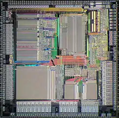
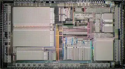
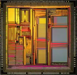
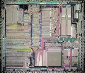
- Die photos
 Am29000
 Am29030
 Am29040
 Am29050
Products and applications
Positioned as a product for "medium- to high-performance embedded applications" with potential for use in Unix workstations,[6] the 29000 was used in a variety of products such as X terminals, laser printer controller cards, graphics accelerator cards, optical character recognition solutions, and network bridges.[20] The memory architecture of the 29000 was a particular attraction for product designers, allowing them to forego external cache memory and to employ dynamic RAM directly while maintaining acceptable performance,[20]: 1 permitting a degree of flexibility in the choice of memory technologies used to retain program instructions and data.[21]
The 29000 saw some use as a computational accelerator or coprocessor, particularly on the Macintosh and IBM PC-compatible platforms. For instance, Yarc Systems Corporation produced 29000-based "RISC coprocessor" cards for Macintosh II and PC AT systems, alongside other "CISC coprocessor" cards featuring Motorola 68020 and 68030 processors, and "parallel coprocessor" cards featuring T800 transputer processors.[22] Its NuSuper (originally named the McCray[23]) and AT-Super cards, employing the Am29000 CPU and Am29027 floating-point accelerator,[22] were followed by the MacRageous, upgrading the CPU to the Am29050.[24] Such accelerator cards offered performance several times that of the Macintosh II itself and benchmarked competitively with RISC workstations such as the DECstation 3100. Multiple cards could also be fitted to a system. However, the cost of a Macintosh II system combined with such a card approached that of established RISC workstations running Unix.[25]
One notable product utilising the 29000 was Apple's Macintosh Display Card 8·24 GC for its Macintosh IIfx, featuring a 30 MHz Am29000 processor, 64 KB static RAM cache, and 2 MB of video RAM, with the option of an additional 2 MB of dynamic RAM for use by the QuickDraw graphical toolkit. The inclusion of the 29000 differentiated this particular version of the card from other versions sold by Apple, significantly improving performance when handling 24-bits-per-pixel images.[26]
References
- Martin, James A. (23 March 1987). "Firm says 32-bit chip handles 17 MIPS". Computerworld. Vol. 21, no. 12. p. 14.
- Cole, Bernard C. (28 April 1988). "RISC Slugfest: Is Marketing More Important Than Performance?" (PDF). Electronics. p. 66 (p. 68 of .pdf).
- "Oral History of William Michael 'Mike' Johnson" (PDF). Computer History Museum (Interview). Interviewed by Kevin Krewell. 9 May 2014.
Well, it started in '85. And it took I would say about three years and maybe four revs till it was functional.
- Betker, Michael R.; Fernando, John S.; Whalen, Shaun P. (Autumn 1997). "The History of the Microprocessor" (PDF). Bell Labs Technical Journal: 48.
- Stewart, Brett (1990). "New generations of the 29 K family solutions". Digest of Papers Compcon Spring '90. Thirty-Fifth IEEE Computer Society International Conference on Intellectual Leverage. pp. 295–298. doi:10.1109/CMPCON.1990.63690.
- Mann, Daniel (October 1991). "Unix and the Am29000 Microprocessor". IEEE Micro. pp. 23–31. ISSN 0272-1732. Retrieved 19 May 2023.
- Mann, Daniel (1995). Evaluating and Programming the 29K™ RISC Family. Advanced Micro Devices. Retrieved 19 May 2023.
- Fickel, Louise (13 May 1991). "Advanced Micro Devices Bolsters 29000 Family With Two RISC CPUs". InfoWorld. Vol. 13, no. 19. p. 28.
- "FLASH MEMORY ANNOUNCEMENTS". Computer Business Review archive at Tech Monitor. 9 October 1990.
- "Am29050™ Microprocessor User's Manual". archive.org. 1991.
- Ganapathy, Gopi; Abraham, Jacob A. Hardware Acceleration Alone Will Not Make Fault Grading ULSI A Reality. International Test Conference 1991.
- Lynch, Thomas Walker; Swartzlander (Jr), Earl E. (July 1991). "The redundant cell adder". Proceedings, 10th IEEE Symposium on Computer Arithmetic. doi:10.1109/ARITH.1991.145553.
- "Am29040 High-Performance RISC Microprocessor with Instruction and Data Caches" (PDF). chipdb.org. Retrieved 18 September 2022.
- Gwennap, Linley. "Digital, MIPS Add Multimedia Extensions" (PDF). Microprocessor Report. 10 (15): 24–28.
- Microprocessor Forum folder. 1994.
{{cite book}}:|website=ignored (help) - McMinn, Brian (14 August 1995). "The First Superscalar 29K Family Member" (PDF). Hot Chips.
- "FIRST SUPERSCALAR Am29000 REVEALED". Computer Business Review archive at Tech Monitor. 28 November 1994.
- Detar, Jim (31 October 1994). "AMD brews up Superscalar 29K". Electronic News.
- Slater, Michael (24 October 1994). "AMD's K5 Designed to Outrun Pentium" (PDF). Microprocessor Report. 8 (14): 1–7.
- FUSIONews 29K. Advanced Micro Devices. Summer 1990. Retrieved 20 May 2023.
- Marshall, Trevor (May 1988). "Real-World RISCs". Byte. pp. 263–268. Retrieved 20 May 2023.
- YARC, the solutions company. Yarc Systems Corporation.
- "YARC Claims 50-MHz Operation for Mac II Booster Board". Byte. August 1988. p. 16. Retrieved 20 May 2023.
- MacRageous Macintosh-II RISC Coprocessor System. Yarc Systems Corporation.
- Varhol, Peter D. (October 1989). "YARC's NuSuper Soups Up the Mac". MIPS. pp. 81–83. Retrieved 20 May 2023.
- Smith, Bud E. (May 1990). "A Big, Fast, Macintosh with RISC Graphics". Personal Workstation. pp. 46–50. Retrieved 20 May 2023.
External links
- AMD 29k (Streamlined Instruction Processor) ID Guide
- Mann, Daniel (1995), Evaluating and Programming the 29K RISC Family (PDF), Advanced Micro Devices, archived from the original (PDF) on September 27, 2007 pdf book about 29k family
- chipdb.org Images of different Am29000 processors