Heterogeneous System Architecture
Heterogeneous System Architecture (HSA) is a cross-vendor set of specifications that allow for the integration of central processing units and graphics processors on the same bus, with shared memory and tasks.[1] The HSA is being developed by the HSA Foundation, which includes (among many others) AMD and ARM. The platform's stated aim is to reduce communication latency between CPUs, GPUs and other compute devices, and make these various devices more compatible from a programmer's perspective,[2]: 3 [3] relieving the programmer of the task of planning the moving of data between devices' disjoint memories (as must currently be done with OpenCL or CUDA).[4]
CUDA and OpenCL as well as most other fairly advanced programming languages can use HSA to increase their execution performance.[5] Heterogeneous computing is widely used in system-on-chip devices such as tablets, smartphones, other mobile devices, and video game consoles.[6] HSA allows programs to use the graphics processor for floating point calculations without separate memory or scheduling.[7]
Rationale
The rationale behind HSA is to ease the burden on programmers when offloading calculations to the GPU. Originally driven solely by AMD and called the FSA, the idea was extended to encompass processing units other than GPUs, such as other manufacturers' DSPs, as well.
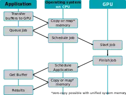 Steps performed when offloading calculations to the GPU on a non-HSA system
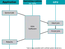 Steps performed when offloading calculations to the GPU on a HSA system, using the HSA functionality
Modern GPUs are very well suited to perform single instruction, multiple data (SIMD) and single instruction, multiple threads (SIMT), while modern CPUs are still being optimized for branching. etc.
Overview
Originally introduced by embedded systems such as the Cell Broadband Engine, sharing system memory directly between multiple system actors makes heterogeneous computing more mainstream. Heterogeneous computing itself refers to systems that contain multiple processing units – central processing units (CPUs), graphics processing units (GPUs), digital signal processors (DSPs), or any type of application-specific integrated circuits (ASICs). The system architecture allows any accelerator, for instance a graphics processor, to operate at the same processing level as the system's CPU.
Among its main features, HSA defines a unified virtual address space for compute devices: where GPUs traditionally have their own memory, separate from the main (CPU) memory, HSA requires these devices to share page tables so that devices can exchange data by sharing pointers. This is to be supported by custom memory management units.[2]: 6–7 To render interoperability possible and also to ease various aspects of programming, HSA is intended to be ISA-agnostic for both CPUs and accelerators, and to support high-level programming languages.
So far, the HSA specifications cover:
HSA Intermediate Layer
HSAIL (Heterogeneous System Architecture Intermediate Language), a virtual instruction set for parallel programs
- similar to LLVM Intermediate Representation and SPIR (used by OpenCL and Vulkan)
- finalized to a specific instruction set by a JIT compiler
- make late decisions on which core(s) should run a task
- explicitly parallel
- supports exceptions, virtual functions and other high-level features
- debugging support
HSA memory model
- compatible with C++11, OpenCL, Java and .NET memory models
- relaxed consistency
- designed to support both managed languages (e.g. Java) and unmanaged languages (e.g. C)
- will make it much easier to develop 3rd-party compilers for a wide range of heterogeneous products programmed in Fortran, C++, C++ AMP, Java, et al.
HSA dispatcher and run-time
- designed to enable heterogeneous task queueing: a work queue per core, distribution of work into queues, load balancing by work stealing
- any core can schedule work for any other, including itself
- significant reduction of overhead of scheduling work for a core
Mobile devices are one of the HSA's application areas, in which it yields improved power efficiency.[6]
Block diagrams
The illustrations below compare CPU-GPU coordination under HSA versus under traditional architectures.
 Standard architecture with a discrete GPU attached to the PCI Express bus. Zero-copy between the GPU and CPU is not possible due to distinct physical memories.
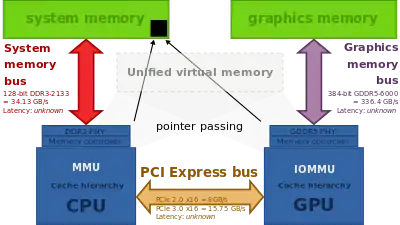 HSA brings unified virtual memory and facilitates passing pointers over PCI Express instead of copying the entire data.
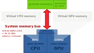 In partitioned main memory, one part of the system memory is exclusively allocated to the GPU. As a result, zero-copy operation is not possible.
 Unified main memory, where GPU and CPU are HSA-enabled. This makes zero-copy operation possible.[8]
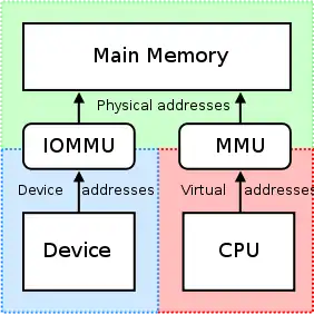
Software support
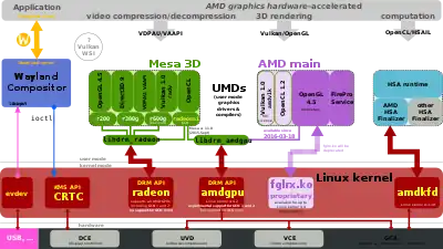
Some of the HSA-specific features implemented in the hardware need to be supported by the operating system kernel and specific device drivers. For example, support for AMD Radeon and AMD FirePro graphics cards, and APUs based on Graphics Core Next (GCN), was merged into version 3.19 of the Linux kernel mainline, released on 8 February 2015.[10] Programs do not interact directly with amdkfd, but queue their jobs utilizing the HSA runtime.[11] This very first implementation, known as amdkfd, focuses on "Kaveri" or "Berlin" APUs and works alongside the existing Radeon kernel graphics driver.
Additionally, amdkfd supports heterogeneous queuing (HQ), which aims to simplify the distribution of computational jobs among multiple CPUs and GPUs from the programmer's perspective. Support for heterogeneous memory management (HMM), suited only for graphics hardware featuring version 2 of the AMD's IOMMU, was accepted into the Linux kernel mainline version 4.14.[12]
Integrated support for HSA platforms has been announced for the "Sumatra" release of OpenJDK, due in 2015.[13]
AMD APP SDK is AMD's proprietary software development kit targeting parallel computing, available for Microsoft Windows and Linux. Bolt is a C++ template library optimized for heterogeneous computing.[14]
GPUOpen comprehends a couple of other software tools related to HSA. CodeXL version 2.0 includes an HSA profiler.[15]
Hardware support
AMD
As of February 2015, only AMD's "Kaveri" A-series APUs (cf. "Kaveri" desktop processors and "Kaveri" mobile processors) and Sony's PlayStation 4 allowed the integrated GPU to access memory via version 2 of the AMD's IOMMU. Earlier APUs (Trinity and Richland) included the version 2 IOMMU functionality, but only for use by an external GPU connected via PCI Express.
Post-2015 Carrizo and Bristol Ridge APUs also include the version 2 IOMMU functionality for the integrated GPU.
The following table shows features of AMD's processors with 3D graphics, including APUs (see also: List of AMD processors with 3D graphics).
| Platform | High, standard and low power | Low and ultra-low power | |||||||||||||||||||||||||||||||||||||||||||||||||||||||||||||||||||||||||||||||||||||||||||||||||||
|---|---|---|---|---|---|---|---|---|---|---|---|---|---|---|---|---|---|---|---|---|---|---|---|---|---|---|---|---|---|---|---|---|---|---|---|---|---|---|---|---|---|---|---|---|---|---|---|---|---|---|---|---|---|---|---|---|---|---|---|---|---|---|---|---|---|---|---|---|---|---|---|---|---|---|---|---|---|---|---|---|---|---|---|---|---|---|---|---|---|---|---|---|---|---|---|---|---|---|---|---|---|
| Codename | Server | Basic | Toronto | ||||||||||||||||||||||||||||||||||||||||||||||||||||||||||||||||||||||||||||||||||||||||||||||||||
| Micro | Kyoto | ||||||||||||||||||||||||||||||||||||||||||||||||||||||||||||||||||||||||||||||||||||||||||||||||||||
| Desktop | Performance | Raphael | |||||||||||||||||||||||||||||||||||||||||||||||||||||||||||||||||||||||||||||||||||||||||||||||||||
| Mainstream | Llano | Trinity | Richland | Kaveri | Kaveri Refresh (Godavari) | Carrizo | Bristol Ridge | Raven Ridge | Picasso | Renoir | Cezanne | ||||||||||||||||||||||||||||||||||||||||||||||||||||||||||||||||||||||||||||||||||||||||||
| Entry | |||||||||||||||||||||||||||||||||||||||||||||||||||||||||||||||||||||||||||||||||||||||||||||||||||||
| Basic | Kabini | Dalí | |||||||||||||||||||||||||||||||||||||||||||||||||||||||||||||||||||||||||||||||||||||||||||||||||||
| Mobile | Performance | Renoir | Cezanne | Rembrandt | Dragon Range | ||||||||||||||||||||||||||||||||||||||||||||||||||||||||||||||||||||||||||||||||||||||||||||||||
| Mainstream | Llano | Trinity | Richland | Kaveri | Carrizo | Bristol Ridge | Raven Ridge | Picasso | Renoir Lucienne |
Cezanne Barceló |
Phoenix | ||||||||||||||||||||||||||||||||||||||||||||||||||||||||||||||||||||||||||||||||||||||||||
| Entry | Dalí | Mendocino | |||||||||||||||||||||||||||||||||||||||||||||||||||||||||||||||||||||||||||||||||||||||||||||||||||
| Basic | Desna, Ontario, Zacate | Kabini, Temash | Beema, Mullins | Carrizo-L | Stoney Ridge | Pollock | |||||||||||||||||||||||||||||||||||||||||||||||||||||||||||||||||||||||||||||||||||||||||||||||
| Embedded | Trinity | Bald Eagle | Merlin Falcon, Brown Falcon |
Great Horned Owl | Grey Hawk | Ontario, Zacate | Kabini | Steppe Eagle, Crowned Eagle, LX-Family |
Prairie Falcon | Banded Kestrel | River Hawk | ||||||||||||||||||||||||||||||||||||||||||||||||||||||||||||||||||||||||||||||||||||||||||
| Released | Aug 2011 | Oct 2012 | Jun 2013 | Jan 2014 | 2015 | Jun 2015 | Jun 2016 | Oct 2017 | Jan 2019 | Mar 2020 | Jan 2021 | Jan 2022 | Sep 2022 | Jan 2023 | Jan 2011 | May 2013 | Apr 2014 | May 2015 | Feb 2016 | Apr 2019 | Jul 2020 | Jun 2022 | Nov 2022 | ||||||||||||||||||||||||||||||||||||||||||||||||||||||||||||||||||||||||||||||
| CPU microarchitecture | K10 | Piledriver | Steamroller | Excavator | "Excavator+"[16] | Zen | Zen+ | Zen 2 | Zen 3 | Zen 3+ | Zen 4 | Bobcat | Jaguar | Puma | Puma+[17] | "Excavator+" | Zen | Zen+ | "Zen 2+" | ||||||||||||||||||||||||||||||||||||||||||||||||||||||||||||||||||||||||||||||||||
| ISA | x86-64 v1 | x86-64 v2 | x86-64 v3 | x86-64 v4 | x86-64 v1 | x86-64 v2 | x86-64 v3 | ||||||||||||||||||||||||||||||||||||||||||||||||||||||||||||||||||||||||||||||||||||||||||||||
| Socket | Desktop | Performance | — | AM5 | — | — | |||||||||||||||||||||||||||||||||||||||||||||||||||||||||||||||||||||||||||||||||||||||||||||||
| Mainstream | — | AM4 | — | — | |||||||||||||||||||||||||||||||||||||||||||||||||||||||||||||||||||||||||||||||||||||||||||||||||
| Entry | FM1 | FM2 | FM2+ | FM2+[lower-alpha 1], AM4 | AM4 | — | |||||||||||||||||||||||||||||||||||||||||||||||||||||||||||||||||||||||||||||||||||||||||||||||
| Basic | — | — | AM1 | — | FP5 | — | |||||||||||||||||||||||||||||||||||||||||||||||||||||||||||||||||||||||||||||||||||||||||||||||
| Other | FS1 | FS1+, FP2 | FP3 | FP4 | FP5 | FP6 | FP7 | FL1 | FP7 FP7r2 FP8 |
? | FT1 | FT3 | FT3b | FP4 | FP5 | FT5 | FP5 | FT6 | |||||||||||||||||||||||||||||||||||||||||||||||||||||||||||||||||||||||||||||||||||
| PCI Express version | 2.0 | 3.0 | 4.0 | 5.0 | 4.0 | 2.0 | 3.0 | ||||||||||||||||||||||||||||||||||||||||||||||||||||||||||||||||||||||||||||||||||||||||||||||
| CXL | — | — | |||||||||||||||||||||||||||||||||||||||||||||||||||||||||||||||||||||||||||||||||||||||||||||||||||
| Fab. (nm) | GF 32SHP (HKMG SOI) |
GF 28SHP (HKMG bulk) |
GF 14LPP (FinFET bulk) |
GF 12LP (FinFET bulk) |
TSMC N7 (FinFET bulk) |
TSMC N6 (FinFET bulk) |
CCD: TSMC N5 (FinFET bulk) cIOD: TSMC N6 (FinFET bulk) |
TSMC 4nm (FinFET bulk) |
TSMC N40 (bulk) |
TSMC N28 (HKMG bulk) |
GF 28SHP (HKMG bulk) |
GF 14LPP (FinFET bulk) |
GF 12LP (FinFET bulk) |
TSMC N6 (FinFET bulk) | |||||||||||||||||||||||||||||||||||||||||||||||||||||||||||||||||||||||||||||||||||||||
| Die area (mm2) | 228 | 246 | 245 | 245 | 250 | 210[18] | 156 | 180 | 210 | CCD: (2x) 70 cIOD: 122 |
178 | 75 (+ 28 FCH) | 107 | ? | 125 | 149 | ~100 | ||||||||||||||||||||||||||||||||||||||||||||||||||||||||||||||||||||||||||||||||||||
| Min TDP (W) | 35 | 17 | 12 | 10 | 15 | 105 | 35 | 4.5 | 4 | 3.95 | 10 | 6 | 12 | 8 | |||||||||||||||||||||||||||||||||||||||||||||||||||||||||||||||||||||||||||||||||||||||
| Max APU TDP (W) | 100 | 95 | 65 | 45 | 170 | 54 | 18 | 25 | 6 | 54 | 15 | ||||||||||||||||||||||||||||||||||||||||||||||||||||||||||||||||||||||||||||||||||||||||||
| Max stock APU base clock (GHz) | 3 | 3.8 | 4.1 | 4.1 | 3.7 | 3.8 | 3.6 | 3.7 | 3.8 | 4.0 | 3.3 | 4.7 | 4.3 | 1.75 | 2.2 | 2 | 2.2 | 3.2 | 2.6 | 1.2 | 3.35 | 2.8 | |||||||||||||||||||||||||||||||||||||||||||||||||||||||||||||||||||||||||||||||
| Max APUs per node[lower-alpha 2] | 1 | 1 | |||||||||||||||||||||||||||||||||||||||||||||||||||||||||||||||||||||||||||||||||||||||||||||||||||
| Max core dies per CPU | 1 | 2 | 1 | 1 | |||||||||||||||||||||||||||||||||||||||||||||||||||||||||||||||||||||||||||||||||||||||||||||||||
| Max CCX per core die | 1 | 2 | 1 | 1 | |||||||||||||||||||||||||||||||||||||||||||||||||||||||||||||||||||||||||||||||||||||||||||||||||
| Max cores per CCX | 4 | 8 | 2 | 4 | 2 | 4 | |||||||||||||||||||||||||||||||||||||||||||||||||||||||||||||||||||||||||||||||||||||||||||||||
| Max CPU[lower-alpha 3] cores per APU | 4 | 8 | 16 | 8 | 2 | 4 | 2 | 4 | |||||||||||||||||||||||||||||||||||||||||||||||||||||||||||||||||||||||||||||||||||||||||||||
| Max threads per CPU core | 1 | 2 | 1 | 2 | |||||||||||||||||||||||||||||||||||||||||||||||||||||||||||||||||||||||||||||||||||||||||||||||||
| Integer pipeline structure | 3+3 | 2+2 | 4+2 | 4+2+1 | 1+3+3+1+2 | 1+1+1+1 | 2+2 | 4+2 | 4+2+1 | ||||||||||||||||||||||||||||||||||||||||||||||||||||||||||||||||||||||||||||||||||||||||||||
| i386, i486, i586, CMOV, NOPL, i686, PAE, NX bit, CMPXCHG16B, AMD-V, RVI, ABM, and 64-bit LAHF/SAHF | |||||||||||||||||||||||||||||||||||||||||||||||||||||||||||||||||||||||||||||||||||||||||||||||||||||
| IOMMU[lower-alpha 4] | — | v2 | v1 | v2 | |||||||||||||||||||||||||||||||||||||||||||||||||||||||||||||||||||||||||||||||||||||||||||||||||
| BMI1, AES-NI, CLMUL, and F16C | — | ||||||||||||||||||||||||||||||||||||||||||||||||||||||||||||||||||||||||||||||||||||||||||||||||||||
| MOVBE | — | ||||||||||||||||||||||||||||||||||||||||||||||||||||||||||||||||||||||||||||||||||||||||||||||||||||
| AVIC, BMI2, RDRAND, and MWAITX/MONITORX | — | ||||||||||||||||||||||||||||||||||||||||||||||||||||||||||||||||||||||||||||||||||||||||||||||||||||
| SME[lower-alpha 5], TSME[lower-alpha 5], ADX, SHA, RDSEED, SMAP, SMEP, XSAVEC, XSAVES, XRSTORS, CLFLUSHOPT, CLZERO, and PTE Coalescing | — | — | |||||||||||||||||||||||||||||||||||||||||||||||||||||||||||||||||||||||||||||||||||||||||||||||||||
| GMET, WBNOINVD, CLWB, QOS, PQE-BW, RDPID, RDPRU, and MCOMMIT | — | — | |||||||||||||||||||||||||||||||||||||||||||||||||||||||||||||||||||||||||||||||||||||||||||||||||||
| MPK, VAES | — | — | |||||||||||||||||||||||||||||||||||||||||||||||||||||||||||||||||||||||||||||||||||||||||||||||||||
| SGX | — | — | |||||||||||||||||||||||||||||||||||||||||||||||||||||||||||||||||||||||||||||||||||||||||||||||||||
| FPUs per core | 1 | 0.5 | 1 | 1 | 0.5 | 1 | |||||||||||||||||||||||||||||||||||||||||||||||||||||||||||||||||||||||||||||||||||||||||||||||
| Pipes per FPU | 2 | 2 | |||||||||||||||||||||||||||||||||||||||||||||||||||||||||||||||||||||||||||||||||||||||||||||||||||
| FPU pipe width | 128-bit | 256-bit | 80-bit | 128-bit | 256-bit | ||||||||||||||||||||||||||||||||||||||||||||||||||||||||||||||||||||||||||||||||||||||||||||||||
| CPU instruction set SIMD level | SSE4a[lower-alpha 6] | AVX | AVX2 | AVX-512 | SSSE3 | AVX | AVX2 | ||||||||||||||||||||||||||||||||||||||||||||||||||||||||||||||||||||||||||||||||||||||||||||||
| 3DNow! | 3DNow!+ | — | — | ||||||||||||||||||||||||||||||||||||||||||||||||||||||||||||||||||||||||||||||||||||||||||||||||||
| PREFETCH/PREFETCHW | |||||||||||||||||||||||||||||||||||||||||||||||||||||||||||||||||||||||||||||||||||||||||||||||||||||
| GFNI | — | — | |||||||||||||||||||||||||||||||||||||||||||||||||||||||||||||||||||||||||||||||||||||||||||||||||||
| AMX | — | ||||||||||||||||||||||||||||||||||||||||||||||||||||||||||||||||||||||||||||||||||||||||||||||||||||
| FMA4, LWP, TBM, and XOP | — | — | — | — | |||||||||||||||||||||||||||||||||||||||||||||||||||||||||||||||||||||||||||||||||||||||||||||||||
| FMA3 | |||||||||||||||||||||||||||||||||||||||||||||||||||||||||||||||||||||||||||||||||||||||||||||||||||||
| AMD XDNA | — | — | |||||||||||||||||||||||||||||||||||||||||||||||||||||||||||||||||||||||||||||||||||||||||||||||||||
| L1 data cache per core (KiB) | 64 | 16 | 32 | 32 | |||||||||||||||||||||||||||||||||||||||||||||||||||||||||||||||||||||||||||||||||||||||||||||||||
| L1 data cache associativity (ways) | 2 | 4 | 8 | 8 | |||||||||||||||||||||||||||||||||||||||||||||||||||||||||||||||||||||||||||||||||||||||||||||||||
| L1 instruction caches per core | 1 | 0.5 | 1 | 1 | 0.5 | 1 | |||||||||||||||||||||||||||||||||||||||||||||||||||||||||||||||||||||||||||||||||||||||||||||||
| Max APU total L1 instruction cache (KiB) | 256 | 128 | 192 | 256 | 512 | 256 | 64 | 128 | 96 | 128 | |||||||||||||||||||||||||||||||||||||||||||||||||||||||||||||||||||||||||||||||||||||||||||
| L1 instruction cache associativity (ways) | 2 | 3 | 4 | 8 | 2 | 3 | 4 | 8 | |||||||||||||||||||||||||||||||||||||||||||||||||||||||||||||||||||||||||||||||||||||||||||||
| L2 caches per core | 1 | 0.5 | 1 | 1 | 0.5 | 1 | |||||||||||||||||||||||||||||||||||||||||||||||||||||||||||||||||||||||||||||||||||||||||||||||
| Max APU total L2 cache (MiB) | 4 | 2 | 4 | 16 | 1 | 2 | 1 | 2 | |||||||||||||||||||||||||||||||||||||||||||||||||||||||||||||||||||||||||||||||||||||||||||||
| L2 cache associativity (ways) | 16 | 8 | 16 | 8 | |||||||||||||||||||||||||||||||||||||||||||||||||||||||||||||||||||||||||||||||||||||||||||||||||
| Max on--die L3 cache per CCX (MiB) | — | 4 | 16 | 32 | — | 4 | |||||||||||||||||||||||||||||||||||||||||||||||||||||||||||||||||||||||||||||||||||||||||||||||
| Max 3D V-Cache per CCD (MiB) | — | 64 | — | — | |||||||||||||||||||||||||||||||||||||||||||||||||||||||||||||||||||||||||||||||||||||||||||||||||
| Max total in-CCD L3 cache per APU (MiB) | 4 | 8 | 16 | 64 | 4 | ||||||||||||||||||||||||||||||||||||||||||||||||||||||||||||||||||||||||||||||||||||||||||||||||
| Max. total 3D V-Cache per APU (MiB) | — | 64 | — | — | |||||||||||||||||||||||||||||||||||||||||||||||||||||||||||||||||||||||||||||||||||||||||||||||||
| Max. board L3 cache per APU (MiB) | — | — | |||||||||||||||||||||||||||||||||||||||||||||||||||||||||||||||||||||||||||||||||||||||||||||||||||
| Max total L3 cache per APU (MiB) | 4 | 8 | 16 | 128 | 4 | ||||||||||||||||||||||||||||||||||||||||||||||||||||||||||||||||||||||||||||||||||||||||||||||||
| APU L3 cache associativity (ways) | 16 | 16 | |||||||||||||||||||||||||||||||||||||||||||||||||||||||||||||||||||||||||||||||||||||||||||||||||||
| L3 cache scheme | Victim | Victim | |||||||||||||||||||||||||||||||||||||||||||||||||||||||||||||||||||||||||||||||||||||||||||||||||||
| Max. L4 cache | — | — | |||||||||||||||||||||||||||||||||||||||||||||||||||||||||||||||||||||||||||||||||||||||||||||||||||
| Max stock DRAM support | DDR3-1866 | DDR3-2133 | DDR3-2133, DDR4-2400 | DDR4-2400 | DDR4-2933 | DDR4-3200, LPDDR4-4266 | DDR5-4800, LPDDR5-6400 | DDR5-5200 | DDR5-5600, LPDDR5x-7500 | DDR3L-1333 | DDR3L-1600 | DDR3L-1866 | DDR3-1866, DDR4-2400 | DDR4-2400 | DDR4-1600 | DDR4-3200 | LPDDR5-5500 | ||||||||||||||||||||||||||||||||||||||||||||||||||||||||||||||||||||||||||||||||||||
| Max DRAM channels per APU | 2 | 1 | 2 | 1 | 2 | ||||||||||||||||||||||||||||||||||||||||||||||||||||||||||||||||||||||||||||||||||||||||||||||||
| Max stock DRAM bandwidth (GB/s) per APU | 29.866 | 34.132 | 38.400 | 46.932 | 68.256 | 102.400 | 83.200 | 120.000 | 10.666 | 12.800 | 14.933 | 19.200 | 38.400 | 12.800 | 51.200 | 88.000 | |||||||||||||||||||||||||||||||||||||||||||||||||||||||||||||||||||||||||||||||||||||
| GPU microarchitecture | TeraScale 2 (VLIW5) | TeraScale 3 (VLIW4) | GCN 2nd gen | GCN 3rd gen | GCN 5th gen[19] | RDNA 2 | RDNA 3 | TeraScale 2 (VLIW5) | GCN 2nd gen | GCN 3rd gen[19] | GCN 5th gen | RDNA 2 | |||||||||||||||||||||||||||||||||||||||||||||||||||||||||||||||||||||||||||||||||||||||||
| GPU instruction set | TeraScale instruction set | GCN instruction set | RDNA instruction set | TeraScale instruction set | GCN instruction set | RDNA instruction set | |||||||||||||||||||||||||||||||||||||||||||||||||||||||||||||||||||||||||||||||||||||||||||||||
| Max stock GPU base clock (MHz) | 600 | 800 | 844 | 866 | 1108 | 1250 | 1400 | 2100 | 2400 | 400 | 538 | 600 | ? | 847 | 900 | 1200 | 600 | 1300 | 1900 | ||||||||||||||||||||||||||||||||||||||||||||||||||||||||||||||||||||||||||||||||||
| Max stock GPU base GFLOPS[lower-alpha 7] | 480 | 614.4 | 648.1 | 886.7 | 1134.5 | 1760 | 1971.2 | 2150.4 | 3686.4 | 102.4 | 86 | ? | ? | ? | 345.6 | 460.8 | 230.4 | 1331.2 | 486.4 | ||||||||||||||||||||||||||||||||||||||||||||||||||||||||||||||||||||||||||||||||||
| 3D engine[lower-alpha 8] | Up to 400:20:8 | Up to 384:24:6 | Up to 512:32:8 | Up to 704:44:16[20] | Up to 512:32:8 | 768:48:8 | 128:8:4 | 80:8:4 | 128:8:4 | Up to 192:12:8 | Up to 192:12:4 | 192:12:4 | Up to 512:?:? | 128:?:? | |||||||||||||||||||||||||||||||||||||||||||||||||||||||||||||||||||||||||||||||||||||||
| IOMMUv1 | IOMMUv2 | IOMMUv1 | ? | IOMMUv2 | |||||||||||||||||||||||||||||||||||||||||||||||||||||||||||||||||||||||||||||||||||||||||||||||||
| Video decoder | UVD 3.0 | UVD 4.2 | UVD 6.0 | VCN 1.0[21] | VCN 2.1[22] | VCN 2.2[22] | VCN 3.1 | ? | UVD 3.0 | UVD 4.0 | UVD 4.2 | UVD 6.0 | UVD 6.3 | VCN 1.0 | VCN 3.1 | ||||||||||||||||||||||||||||||||||||||||||||||||||||||||||||||||||||||||||||||||||||||
| Video encoder | — | VCE 1.0 | VCE 2.0 | VCE 3.1 | — | VCE 2.0 | VCE 3.1 | ||||||||||||||||||||||||||||||||||||||||||||||||||||||||||||||||||||||||||||||||||||||||||||||
| AMD Fluid Motion | |||||||||||||||||||||||||||||||||||||||||||||||||||||||||||||||||||||||||||||||||||||||||||||||||||||
| GPU power saving | PowerPlay | PowerTune | PowerPlay | PowerTune[23] | |||||||||||||||||||||||||||||||||||||||||||||||||||||||||||||||||||||||||||||||||||||||||||||||||
| TrueAudio | — | ? | — | ||||||||||||||||||||||||||||||||||||||||||||||||||||||||||||||||||||||||||||||||||||||||||||||||||
| FreeSync | 1 2 |
1 2 | |||||||||||||||||||||||||||||||||||||||||||||||||||||||||||||||||||||||||||||||||||||||||||||||||||
| HDCP[lower-alpha 9] | ? | 1.4 | 2.2 | 2.3 | ? | 1.4 | 2.2 | 2.3 | |||||||||||||||||||||||||||||||||||||||||||||||||||||||||||||||||||||||||||||||||||||||||||||
| PlayReady[lower-alpha 9] | — | 3.0 not yet | — | 3.0 not yet | |||||||||||||||||||||||||||||||||||||||||||||||||||||||||||||||||||||||||||||||||||||||||||||||||
| Supported displays[lower-alpha 10] | 2–3 | 2–4 | 3 | 3 (desktop) 4 (mobile, embedded) | 4 | 2 | 3 | 4 | 4 | ||||||||||||||||||||||||||||||||||||||||||||||||||||||||||||||||||||||||||||||||||||||||||||
/drm/radeon[lower-alpha 11][26][27] | — | — | |||||||||||||||||||||||||||||||||||||||||||||||||||||||||||||||||||||||||||||||||||||||||||||||||||
/drm/amdgpu[lower-alpha 11][28] | — | — | |||||||||||||||||||||||||||||||||||||||||||||||||||||||||||||||||||||||||||||||||||||||||||||||||||
- For FM2+ Excavator models: A8-7680, A6-7480 & Athlon X4 845.
- A PC would be one node.
- An APU combines a CPU and a GPU. Both have cores.
- Requires firmware support.
- Requires firmware support.
- No SSE4. No SSSE3.
- Single-precision performance is calculated from the base (or boost) core clock speed based on a FMA operation.
- Unified shaders : texture mapping units : render output units
- To play protected video content, it also requires card, operating system, driver, and application support. A compatible HDCP display is also needed for this. HDCP is mandatory for the output of certain audio formats, placing additional constraints on the multimedia setup.
- To feed more than two displays, the additional panels must have native DisplayPort support.[25] Alternatively active DisplayPort-to-DVI/HDMI/VGA adapters can be employed.
- DRM (Direct Rendering Manager) is a component of the Linux kernel. Support in this table refers to the most current version.
See also
References
- Tarun Iyer (30 April 2013). "AMD Unveils its Heterogeneous Uniform Memory Access (hUMA) Technology". Tom's Hardware.
- George Kyriazis (30 August 2012). Heterogeneous System Architecture: A Technical Review (PDF) (Report). AMD. Archived from the original (PDF) on 28 March 2014. Retrieved 26 May 2014.
- "What is Heterogeneous System Architecture (HSA)?". AMD. Archived from the original on 21 June 2014. Retrieved 23 May 2014.
- Joel Hruska (26 August 2013). "Setting HSAIL: AMD explains the future of CPU/GPU cooperation". ExtremeTech. Ziff Davis.
- Linaro (21 March 2014). "LCE13: Heterogeneous System Architecture (HSA) on ARM". slideshare.net.
- "Heterogeneous System Architecture: Purpose and Outlook". gpuscience.com. 9 November 2012. Archived from the original on 1 February 2014. Retrieved 24 May 2014.
- "Heterogeneous system architecture: Multicore image processing using a mix of CPU and GPU elements". Embedded Computing Design. Retrieved 23 May 2014.
- "Kaveri microarchitecture". SemiAccurate. 15 January 2014.
- Michael Larabel (21 July 2014). "AMDKFD Driver Still Evolving For Open-Source HSA On Linux". Phoronix. Retrieved 21 January 2015.
- "Linux kernel 3.19, Section 1.3. HSA driver for AMD GPU devices". kernelnewbies.org. 8 February 2015. Retrieved 12 February 2015.
- "HSA-Runtime-Reference-Source/README.md at master". github.com. 14 November 2014. Retrieved 12 February 2015.
- "Linux Kernel 4.14 Announced with Secure Memory Encryption and More". 13 November 2017.
- Alex Woodie (26 August 2013). "HSA Foundation Aims to Boost Java's GPU Prowess". HPCwire.
- "Bolt on github". GitHub. 11 January 2022.
- AMD GPUOpen (19 April 2016). "CodeXL 2.0 includes HSA profiler". Archived from the original on 27 June 2018. Retrieved 21 April 2016.
- "AMD Announces the 7th Generation APU: Excavator mk2 in Bristol Ridge and Stoney Ridge for Notebooks". 31 May 2016. Retrieved 3 January 2020.
- "AMD Mobile "Carrizo" Family of APUs Designed to Deliver Significant Leap in Performance, Energy Efficiency in 2015" (Press release). 20 November 2014. Retrieved 16 February 2015.
- "The Mobile CPU Comparison Guide Rev. 13.0 Page 5 : AMD Mobile CPU Full List". TechARP.com. Retrieved 13 December 2017.
- "AMD VEGA10 and VEGA11 GPUs spotted in OpenCL driver". VideoCardz.com. Retrieved 6 June 2017.
- Cutress, Ian (1 February 2018). "Zen Cores and Vega: Ryzen APUs for AM4 – AMD Tech Day at CES: 2018 Roadmap Revealed, with Ryzen APUs, Zen+ on 12nm, Vega on 7nm". Anandtech. Retrieved 7 February 2018.
- Larabel, Michael (17 November 2017). "Radeon VCN Encode Support Lands in Mesa 17.4 Git". Phoronix. Retrieved 20 November 2017.
- "AMD Ryzen 5000G 'Cezanne' APU Gets First High-Res Die Shots, 10.7 Billion Transistors In A 180mm2 Package". wccftech. 12 August 2021. Retrieved 25 August 2021.
- Tony Chen; Jason Greaves, "AMD's Graphics Core Next (GCN) Architecture" (PDF), AMD, retrieved 13 August 2016
- "A technical look at AMD's Kaveri architecture". Semi Accurate. Retrieved 6 July 2014.
- "How do I connect three or More Monitors to an AMD Radeon™ HD 5000, HD 6000, and HD 7000 Series Graphics Card?". AMD. Retrieved 8 December 2014.
- Airlie, David (26 November 2009). "DisplayPort supported by KMS driver mainlined into Linux kernel 2.6.33". Retrieved 16 January 2016.
- "Radeon feature matrix". freedesktop.org. Retrieved 10 January 2016.
- Deucher, Alexander (16 September 2015). "XDC2015: AMDGPU" (PDF). Retrieved 16 January 2016.
- Michel Dänzer (17 November 2016). "[ANNOUNCE] xf86-video-amdgpu 1.2.0". lists.x.org.
- "ARM Bifrost GPU Architecture". 30 May 2016.
External links
- HSA Heterogeneous System Architecture Overview on YouTube by Vinod Tipparaju at SC13 in November 2013
- HSA and the software ecosystem
- 2012 – HSA by Michael Houston