GlobalFoundries
GlobalFoundries Inc. (GF) is a multinational semiconductor contract manufacturing and design company incorporated in the Cayman Islands and headquartered in Malta, New York.[4] Created by the divestiture of the manufacturing arm of AMD, the company was privately owned by Mubadala Investment Company, the sovereign wealth fund of the United Arab Emirates, until an initial public offering (IPO) in October 2021.
| Type | Public |
|---|---|
| |
| ISIN | KYG393871085 |
| Industry | Semiconductors |
| Founded | March 2, 2009 (as a spin-off of AMD) |
| Headquarters | Malta, New York, U.S. |
Key people | Ahmed Yahia Al Idrissi (Chairman) Thomas Caulfield (CEO) |
| Services | Semiconductor manufacturer |
| Revenue | |
| Total assets | |
| Total equity | |
Number of employees | 13,000 (2022) |
| Website | gf |
| Footnotes / references [1][2][3] | |
The company manufactures integrated circuits on wafers designed for markets such as smart mobile devices, automotive, aerospace and defense, consumer internet of things (IoT) and for data centers and communications infrastructure.
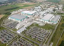
As of 2023, GlobalFoundries is the third-largest semiconductor foundry by revenue.[5] [6][7] It is the only one with operations in Singapore, the European Union, and the United States: one 200 mm and one 300 mm wafer fabrication plant in Singapore; one 300 mm plant in Dresden, Germany; one 200 mm plant in Burlington, Vermont (where it is the largest private employer)[8] and one 300 mm plant in the State of New York: in Malta.[9]
GlobalFoundries is a "Trusted Foundry" for the U.S. federal government and has similar designations in Singapore and Germany, including certified international Common Criteria standard (ISO 15408, CC Version 3.1).[10][11]
On October 28, 2021, the company sold shares in an IPO on the Nasdaq stock exchange at US$47 each, at the higher end of its targeted price range, and raised about US$2.6 billion.[12]
Overview
On October 7, 2008, AMD announced it planned to go fabless and spin off their semiconductor manufacturing business into a new company temporarily called The Foundry Company. Mubadala announced their subsidiary Advanced Technology Investment Company (ATIC) agreed to pay $700 million to increase their stake in AMD's semiconductor manufacturing business to 55.6% (up from 8.1%). Mubadala will invest $314 million for 58 million new shares, increasing their stake in AMD to 19.3%. $1.2 billion of AMD's debt will be transferred to The Foundry Company.[13] On 8 December 2008, amendments were announced. AMD will own approximately 34.2% and ATIC will own approximately 65.8% of The Foundry Company.[14]
On March 4, 2009, GlobalFoundries was officially announced.[15] On September 7, 2009, ATIC announced it would acquire Chartered Semiconductor, based in Singapore, for S$2.5 billion (US$1.8 billion) and integrate Chartered Semiconductor into GlobalFoundries.[16] On January 13, 2010, GlobalFoundries announced it had finalized the integration of Chartered Semiconductor.[17]
On March 4, 2012, AMD announced they divested their final 14% stake in the company, which concluded AMD's multi-year plan to divest its manufacturing arm.[18]
On October 20, 2014, IBM announced the sale of its microelectronics business to GlobalFoundries.[19]
As of 2015, the firm owned ten fabrication plants. Fab 1 is in Dresden, Germany. Fabs 2 through 7 are in Singapore. Fabs 8 through 10 are in the northeast United States. These sites are supported by a global network of R&D, design enablement, and customer support in Singapore, China, Taiwan, Japan, India, the United States, Germany, and the United Kingdom.[20] In February 2017, the company announced a new 300 Fab [Fab 11] in China for growing semiconductor market in China.[21]
In 2016, GlobalFoundries licensed the 14 nm 14LPP FinFET process from Samsung Electronics. In 2018, GlobalFoundries developed the 12 nm 12LP node based on Samsung's 14 nm 14LPP process.[22]
On August 27, 2018, GlobalFoundries announced it had cancelled their 7LP process due to a strategy shift to focus on specialized processes instead of leading edge performance.[23]
On January 29, 2019, AMD announced an amended wafer supply agreement with GlobalFoundries. AMD now has full flexibility for wafer purchases from any foundry at 7 nm or beyond. AMD and GlobalFoundries agreed to commitments and pricing at 12 nm for 2019 through 2021.[24]
On May 20, 2019, Marvell Technology Group announced it would acquire Avera Semi from GlobalFoundries for $650 million and potentially an additional $90 million. Avera Semi was GlobalFoundries' ASIC Solutions division, which had been a part of IBM's semiconductor manufacturing business.[25] On February 1, 2019, GlobalFoundries announced the $236 million sale of its Fab 3E in Tampines, Singapore, to Vanguard International Semiconductor (VIS) as part of their plan to exit the MEMS business by December 31, 2019.[26] On April 22, 2019, GlobalFoundries announced the $430 million sale of their Fab 10 in East Fishkill, New York, to ON Semiconductor. GlobalFoundries has received $100 million and will receive $330 million at the end of 2022 when ON Semiconductor will gain full operational control. The 300mm fab is capable of 65 nm to 40 nm and was a part of IBM.[27] On August 15, 2019, GlobalFoundries announced a multi-year supply agreement with Toppan Photomasks. The agreement included Toppan acquiring GlobalFoundries' Burlington photomask facility.[28]
In February 2020, GlobalFoundries announced that its embedded magnetoresistive non-volatile memory (eMRAM) entered production which is the industry's first production ready eMRAM.[29]
In May 2020, GlobalFoundries stated it was fully abandoning its plans of opening Fab 11 in Chengdu, China due to reported rivalry between the latter and the US.[30] This was three years after the manufacturer announced it would invest $10 billion to open the new fab; the fab was never brought online.[31]
On April 26, 2021, GlobalFoundries announced that effective immediately, it was transferring its global headquarters from Santa Clara, California to its Malta, New York campus (home to Fab 8).[32]
In August 2022, Google expanded its open-source chip design and manufacturing efforts by partnering with GlobalFoundries to develop an open-source process design kit (PDK) based on the foundry's 180 nm node.[33][34] In October 31, Google announced they would sponsor no-cost OpenMPW (multi-project wafer) shuttle runs for it in the coming months.[35]
In February 2023, GlobalFoundries signed a deal to become the exclusive provider of US-produced semiconductor chips for GM amid an ongoing shift to electric vehicles in what was referred to as an "industry-first" deal. It would help GM reduce the amount of different chips needed in its vehicles. The companies planned for production in Malta, New York. The deal would not lead to new jobs right away but would rather ensure stability in the supply of chips. At the time of the announcement, GlobalFoundries CEO Thomas Caufield said the full effect of this increase in production would be seen in two to three years.[36][37][38][39][40]
On September 21, 2023, the U.S. Department of Defense (DoD) awarded GlobalFoundries a 10-year contract for the supply of securely manufactured semiconductors for critical aerospace and defense applications. With an initial award of $17.3 million and an overall 10-year spending ceiling of $3.1 billion, this agreement ensures the DoD and its contractors have access to GF's U.S.-made semiconductors. This contract also provides access to GF's design ecosystem, IP libraries, and advanced technologies.[41]
GlobalFoundries v. TSMC et al (2019)
On August 26, 2019, GlobalFoundries filed patent infringement lawsuits against TSMC and some of TSMC's customers[42] in the US and Germany. GlobalFoundries claims TSMC's 7 nm, 10 nm, 12 nm, 16 nm, and 28 nm nodes have infringed on 16 of its patents. Lawsuits were filed in the U.S. International Trade Commission, the U.S. Federal District Courts in the Districts of Delaware, the Western District of Texas, the Regional Courts of Düsseldorf, and Mannheim in Germany.[43] GlobalFoundries has named 20 defendants: Apple, Broadcom, MediaTek, Nvidia, Qualcomm, Xilinx, Arista, ASUS, BLU, Cisco, Google, Hisense, Lenovo, Motorola, TCL, OnePlus, Avnet/EBV, Digi-Key and Mouser.[44] On August 27, TSMC announced it was reviewing the complaints filed, but are confident that the allegations are baseless and will vigorously defend its proprietary technology.[45]
On October 1, 2019, TSMC filed patent infringement lawsuits against GlobalFoundries in the US, Germany and Singapore. TSMC claimed GlobalFoundries' 12 nm, 14 nm, 22 nm, 28 nm and 40 nm nodes have infringed on 25 of its patents.[46]
On October 29, 2019, TSMC and GlobalFoundries announced a resolution to the dispute. The companies agreed to a new life-of-patents cross-license for all of their existing semiconductor patents as well as new patents to be filed by the companies in the next ten years.[47][48][49][50][51]
List of GlobalFoundries CEOs
- Doug Grose (2009–2011)[52]
- Ajit Manocha (2011–2014)
- Sanjay Jha (2014–2018)[53]
- Tom Caulfield (2018–present)[54]
Fabrication foundries in operation
| Name | Wafer | Location | Process | |
|---|---|---|---|---|
| Fab 1 | 300 mm | Dresden, Germany | 51.125°N 13.716°E | 55, 45, 40, 32, 28, 22 nm, 12 nm |
| Fab 2 | 200 mm | Woodlands, Singapore | 1.436°N 103.766°E | 600–350 nm |
| Fab 3/5 | 200 mm | Woodlands, Singapore | 1.436°N 103.766°E | 350–180 nm |
| Fab 3E | 200 mm | Tampines, Singapore (2019: sold to VIS) | 1.371°N 103.929°E | 180 nm |
| Fab 6 | 200 mm | Woodlands, Singapore (converted to 300 mm and merged into Fab 7) | 1.436°N 103.766°E | 180–110 nm |
| Fab 7 | 300 mm | Woodlands, Singapore | 1.436°N 103.766°E | 130–40 nm |
| Fab 8 | 300 mm | Luther Forest Technology Campus, Saratoga County, New York, United States | 42.970°N 73.756°W | 28, 20, 14 nm |
| Fab 9 | 200 mm | Essex Junction, Vermont, United States | 44.48°N 73.10°W[55] | 350–90 nm |
300 mm fabrication facilities
Fab 1
Fab 1, located in Dresden, Germany, is a 364,512 m2 plant which was transferred to GlobalFoundries on its inception: Fab 36 and Fab 38 were renamed Module 1 and Module 2, respectively. Each module can produce 25,000 300 mm diameter wafers per month.[9][56]
Module 1 is a 300 mm wafer production facility. It is capable of manufacturing wafers at 40 nm, 28 nm BULK and 22 nm FDSOI. Module 2 was originally named "(AMD) Fab 30" and was a 200 mm fab producing 30,000 Wafer Outs Per Month, but has now been converted into a 300 mm wafer fab. Together with other clean room extensions like the Annex they have a maximum full capacity of 80,000 of 300 mm wafers/month (180,000 200 mm wafers/month equivalent), using technologies of 45 nm and below.
In September 2016, GlobalFoundries announced Fab 1 would be refit to produce 12 nm fully depleted silicon on insulator (FDSOI) products.[57] The company expected customer's products would begin to tape out in the first half of 2019.
Fab 7
Fab 7, located in Woodlands, Singapore, is an operational 300 mm Fab, originally owned by Chartered Semiconductor. It produces wafers at 130 nm to 40 nm on bulk CMOS and SOI processes. It has a maximum full capacity of 50,000 300 mm wafers/month (112,500 200 mm wafers/month equivalent), using 130 to 40 nm technology.[9]
4/15/2021 Fab 7's target capacity will be expanded to 70–80kpcs/M.
Fab 8
Fab 8, located in Luther Forest Technology Campus, Saratoga County, New York, United States is a 300 mm fab. This fabrication plant was constructed by GF as a green field fab for advanced technologies. It is capable of manufacturing 14 nm node technology. The plant's construction began in July 2009 and the company started mass production in 2012.[9][58] It has a maximum manufacturing capacity of 60,000 of 300 mm wafers/month, or the equivalent of over 135,000 of 200 mm wafers/month. In September 2016, GlobalFoundries announced it would make a multibillion-dollar investment to refit Fab 8 to produce 7 nm FinFET parts starting in the second half of 2018.[59] The process was planned to initially use deep ultraviolet lithography, and eventually transition to extreme ultraviolet lithography.[60]
However, in August 2018, GlobalFoundries made the decision to suspend 7 nm development and planned production, citing the unaffordable costs to outfit Fab 8 for 7 nm production. GlobalFoundries held open the possibility of resuming 7 nm operations in the future if additional resources could be secured. From this decision GlobalFoundries executed a shift in company strategy to focus more effort on FD-SOI manufacturing and R&D. Fab 8 serves a crucial function to supply AMD (Advanced Micro Devices) with CPU Wafers for its Zen line of microprocessors used in the Ryzen, Threadripper and Epyc lines of CPUs. The original Zen and the Zen+ CPUs are of a monolithic design which were produced at Global Foundries Malta Facilities in Malta, NY. Going forward AMD will pursue a multiple Chiplet Design with the Zen 2 microprocessor. The Zen 2 will consist of a 14/12 nm manufactured IO die surrounded by a number of 7 nm Core dies. When Global Foundries announced the suspension of 7 nm operations AMD executed a shift in plans transferring production of the 7 nm core dies to TSMC (Taiwan Semiconductor Corporation). There was speculation in some quarters as to where manufacture of the Core Dies would take place. In AMD's 2018 fourth quarter financial conference call which took place on January 29, 2019, AMD CEO Lisa Su announced the WSA (Wafer Supply Agreement) governing production and acquisition by AMD from GlobalFoundries had been amended for the seventh time. The amendment stated AMD would continue to procure 12 nm node and above from Global Foundries while giving AMD latitude to purchase 7 nm node manufactured wafers from any source free from paying any royalties. The agreement will run through 2024 and ensures that Global Foundries will have work for its Malta plant for that time period. Pricing commitments for Wafers runs through 2021 when it is likely the WSA will be amended again.[61]
Accreditation as a Trusted Supplier
In May 2023, the U.S. Department of Defense (DoD), through the Defense Microelectronics Activity (DMEA), Trusted Access Program Office (TAPO), accredited GlobalFoundries' advanced manufacturing facility in Malta, New York, as a Category 1A Trusted Supplier. This accreditation enables GlobalFoundries to manufacture secure semiconductors for a wide range of critical aerospace and defense applications.[62]
Fab 10
Fab 10,[63] located in East Fishkill, New York, United States, was previously known as IBM Building 323. It became part of GlobalFoundries operations with the acquisition of IBM Microelectronics. It currently manufactures technology down to the 14 nm node. In April 2019, it was announced that this fab has been sold to ON Semiconductor for $430m. The facility will be transferred over within three years.[64]
On February 10, 2023, onsemi successfully completed its acquisition of GF's 300 mm East Fishkill, New York site and fabrication facility.[65]
200 mm fabrication facilities
All 200 mm fabs except Fab 9 are located in Singapore, and originally owned by Chartered Semiconductor.
Fab 2
Fab 2, located in Woodlands, Singapore. This fab is capable of manufacturing wafers at 600 to 350 nm for use in selected automotive IC products, High Voltage power management IC and Mixed-signal products.
Fab 3/5
Fab 3/5, located in Woodlands, Singapore. This fab is capable of manufacturing wafers at 350 to 180 nm for use in high voltage IC's for small panel display drivers and mobile power management modules.
Fab 3E
Fab 3E, located in Tampines, Singapore. This fab produces 180 nm wafers for use in selected automotive IC products, High Voltage power management IC and Mixed-Signal products with embedded non-volatile memory technology.
In January 2019 GlobalFoundries announced that it had agreed to sell its Fab 3E in Singapore to Vanguard International Semiconductor Corporation with transfer of ownership set to be completed on December 31, 2019.
Fab 6
Fab 6 located in Woodlands, Singapore, is a copper fabrication facility that is capable of manufacturing integrated CMOS and RFCMOS products for applications such as Wi-Fi & Bluetooth devices at 180 to 110 nm processes. The facility was later converted to 300mm and merged with Fab 7, a facility for manufacturing products based on the 300 nm node.
Fab 9
Fab 9,[63] located in the village of Essex Junction, Vermont, United States, near Vermont's largest city of Burlington, became part of GlobalFoundries operations with the acquisition of IBM Microelectronics. The fab manufactures technologies down to the 90 nm node and is the largest private employer within the state of Vermont. The site also hosted a captive mask shop, with development efforts down to the 7 nanometer node, until it was sold to Toppan in 2019.[66]
Mergers and acquisitions
Chartered Semiconductor
The majority investor of GlobalFoundries, Abu Dhabi's Advanced Technology Investment Co., announced on September 6, 2009, that it has agreed to acquire Singapore-based Chartered Semiconductor Manufacturing Co. Ltd., for a total of $3.9 billion, with Chartered's operations being folded into GlobalFoundries.[67]
Chartered Semiconductor is a member of the Common Platform, IBM's semiconductor technology alliance. GlobalFoundries is a JDA partner of Common Platform Technology Alliance.
IBM Microelectronics
In October 2014, GlobalFoundries received US$1.5 billion from IBM to accept taking over IBM Microelectronics, including a 200 mm fab (now Fab 9) in Essex Junction, Vermont, and a 300 mm fab (now Fab 10) in East Fishkill, New York. As part of the agreement, GlobalFoundries will be the sole provider of IBM's server processor chips for the next 10 years. The deal closed on July 1, 2015.[68] IBM-India employees who moved over to GlobalFoundries as part of the acquisition are now part of its Bangalore office.[69]
In April 2019 ON Semiconductor and GlobalFoundries announced a $430 million agreement to transfer ownership of GlobalFoundries 300mm Fab 10 in East Fishkill, New York, to ON Semiconductor.[70]
In 2021 and 2023, GlobalFoundries sued IBM over intellectual property disputes involving the latter's agreements with Intel and Rapidus.[71]
Process technologies
GlobalFoundries' 22 nm FD-SOI process is second-sourced from STMicroelectronics.[72] STMicroelectronics signed a sourcing and licensing agreement with Samsung for the same technology later.[73]
GlobalFoundries' 14 nm 14LPP FinFET process is second-sourced from Samsung Electronics. GlobalFoundries' 12 nm FinFET nodes are based on Samsung's 14 nm 14LPP process.[22]
| Node name | ITRS node (nm) | Date introduced | Wafer size (mm) | Lithography (wavelength) | Transistor type | Gate pitch (nm) | Metal 1 pitch (nm) | SRAM bit density (µm2) |
|---|---|---|---|---|---|---|---|---|
| 4S | 600 | 1993 | 200 Bulk | – | Planar | – | – | – |
| CS-24 | 500 | 1993 | Bulk | – | Planar | – | – | – |
| 5L | 500 | – | 200 Bulk | – | Planar | – | – | – |
| 5S | 500 | 1994 | 200 Bulk | – | Planar | – | – | – |
| SiGe 5HP | 500 | 2001 | 200 | – | Planar | – | – | – |
| SiGe 5AM | 500 | 2001 | 200 | – | Planar | – | – | – |
| SiGe 5DM | 500 | 2002 | 200 | – | Planar | – | – | – |
| SiGe 5PA | 500 | 2002 | 200 | – | Planar | – | – | – |
| 5X | 450 | 1994 | 200 Bulk | – | Planar | – | – | – |
| CS-34 | 350 | 1995 | Bulk | – | Planar | – | – | – |
| SiGe 5HPE | 350 | 2001 | 200 | – | Planar | – | – | – |
| SiGe 5PAe[74] | 350 | 2007 | 200 | – | Planar | – | – | – |
| SiGe 5PAx[74] | 350 | 2016 | 200 | – | Planar | – | – | – |
| SiGe 1KW5PAe[74] | 350 | – | 200 | – | Planar | – | – | – |
| SiGe 1K5PAx[74] | 350 | 2016 | 200 | – | Planar | – | – | – |
| 6S | 290 | 1996 | 200 Bulk | – | Planar | – | – | – |
| CS-44 | 250 | 1998 | Bulk | Dry 248nm DUV | Planar | – | – | – |
| 6S2 | 250 | 1997 | 200 Bulk | Dry 248nm DUV | Planar | – | – | – |
| 6SF | 250 | – | 200 Bulk | Dry 248nm DUV | Planar | – | – | – |
| 6X | 250 | 1997 | 200 Bulk | – | Planar | – | – | – |
| 6RF | 250 | 2001 | 200 Bulk | Dry 248nm DUV | Planar | – | – | – |
| 250SOI | 250 | 1999 | 200 SOI | Dry 248nm DUV | Planar | – | – | – |
| SiGe 6HP | 250 | – | 200 | Dry 248nm DUV | Planar | – | – | – |
| SiGe 6DM | 250 | – | 200 | Dry 248nm DUV | Planar | – | – | – |
| SiGe 6WL | 250 | 2007 | 200 | Dry 248nm DUV | Planar | – | – | – |
| 7S | 220 | 1998 | 200 Bulk | Dry 248nm DUV | Planar | – | – | – |
| 220SOI | 220 | 1999 | 200 SOI | Dry 248nm DUV | Planar | – | – | – |
| 7HV | 180 | 2010 | 200 | Dry 248nm DUV | Planar | – | – | – |
| 180 BCDLite[75] | 180 | 2011 | 200 | Dry 248nm DUV | Planar | – | – | – |
| 180 UHV[75] | 180 | 2017 | 200 | Dry 248nm DUV | Planar | – | – | – |
| 7SF | 180 | 1999 | 200 Bulk | Dry 248nm DUV | Planar | – | – | – |
| 7TG | 180 | – | 200 Bulk | Dry 248nm DUV | Planar | – | – | – |
| 7RF | 180 | 2003 | 200 Bulk | Dry 248nm DUV | Planar | – | – | – |
| 8S | 180 | 2000 | 200 SOI | Dry 248nm DUV | Planar | – | – | – |
| 7RF SOI[76] | 180 | 2007 | 200 RF-SOI, 300 RF-SOI | Dry 248nm DUV | Planar | – | – | – |
| 7SW RF SOI[76] | 180 | 2014 | 200 RF-SOI | Dry 248nm DUV | Planar | – | – | – |
| SiGe 7WL[77] | 180 | 2003 | 200 | Dry 248nm DUV | Planar | – | – | – |
| SiGe 7HP | 180 | 2003 | 200 | Dry 248nm DUV | Planar | – | – | – |
| 130 BCDLite[75] | 130 | 2014 | 300 | Dry 248nm DUV | Planar | – | – | – |
| 130 BCD[75] | 130 | – | 300 | Dry 248nm DUV | Planar | – | – | – |
| 8SF | 130 | 2000 | 200 Bulk | Dry 248nm DUV | Planar | – | – | – |
| 8SFG | 130 | 2003 | 200 Bulk, 300 Bulk | Dry 248nm DUV | Planar | – | – | – |
| 8RF | 130 | 2003 | 200 Bulk, 300 Bulk | Dry 248nm DUV | Planar | – | – | – |
| 130G[78] | 130 | – | 300 Bulk | Dry 248nm DUV | Planar | – | – | – |
| 130LP[78] | 130 | – | 300 Bulk | Dry 248nm DUV | Planar | – | – | – |
| 130LP/EE[78] | 130 | – | 300 Bulk | Dry 248nm DUV | Planar | – | – | – |
| 110TS[78] | 130 | – | 300 Bulk | Dry 248nm DUV | Planar | – | – | – |
| 9S | 130 | 2000 | 200 SOI, 300 SOI | Dry 248nm DUV | Planar | – | – | – |
| 130RFSOI[76] | 130 | 2015 | 300 RF-SOI | Dry 248nm DUV | Planar | – | – | – |
| 8SW RF SOI[76] | 130 | 2017 | 300 RF-SOI | Dry 248nm DUV | Planar | – | – | – |
| SiGe 8WL[77] | 130 | 2005 | 200 | Dry 248nm DUV | Planar | – | – | – |
| SiGe 8HP[77] | 130 | 2005 | 200, 300 | Dry 248nm DUV | Planar | – | – | – |
| SiGe 8XP[77] | 130 | 2016 | 200 | Dry 248nm DUV | Planar | – | – | – |
| 9SF | 90 | 2004 | 300 Bulk | Dry 193nm DUV | Planar | – | – | – |
| 9LP | 90 | 2005 | 300 Bulk | Dry 193nm DUV | Planar | – | – | – |
| 9RF | 90 | – | 300 Bulk | Dry 193nm DUV | Planar | – | – | – |
| 10S | 90 | 2002 | 300 SOI | Dry 193nm DUV | Planar | – | – | – |
| 90RFSOI | 90 | 2004 | 300 RF-SOI | Dry 193nm DUV | Planar | – | – | – |
| 90WG[79] | 90 | 2018 | 300 | Dry 193nm DUV | Planar | – | – | – |
| 90WG+[79] | 90 | ? | 300 | Dry 193nm DUV | Planar | – | – | – |
| SiGe 9HP[77] | 90 | 2014, 2018 | 200, 300 | Dry 193nm DUV | Planar | – | – | – |
| 10SF | 65 | – | 300 Bulk | Dry 193nm DUV | Planar | – | – | – |
| 10LP | 65 | – | 300 Bulk | Dry 193nm DUV | Planar | – | – | – |
| 65LPe[80] | 65 | 2009 | 300 Bulk | Dry 193nm DUV | Planar | – | – | – |
| 65LPe-RF[80] | 65 | 2009 | 300 Bulk | Dry 193nm DUV | Planar | – | – | – |
| 10RFe | 65 | – | 300 Bulk | Dry 193nm DUV | Planar | – | – | – |
| 11S | 65 | 2006 | 300 SOI | Dry 193nm DUV | Planar | – | – | – |
| 65RFSOI | 65 | 2008 | 300 RF-SOI | Dry 193nm DUV | Planar | – | – | – |
| 55 BCDLite[80] | 55 | 2018 | 300 | Dry 193nm DUV | Planar | – | – | – |
| 55HV[81] | 55 | ? | 300 | Dry 193nm DUV | Planar | – | – | – |
| 55 ULP[80] | 55 | – | 300 Bulk | Dry 193nm DUV | Planar | – | – | – |
| 55LPe | 55 | – | 300 Bulk | Dry 193nm DUV | Planar | – | – | – |
| 55LPe-RF | 55 | – | 300 Bulk | Dry 193nm DUV | Planar | – | – | – |
| 55LPx[80] | 55 | – | 300 Bulk | Dry 193nm DUV | Planar | – | – | – |
| 55RF[80] | 55 | – | 300 Bulk | Dry 193nm DUV | Planar | – | – | – |
| 45LP | 45 | – | 300 Bulk | Wet 193nm DUV | Planar | – | – | – |
| 12S | 45 | 2007 | 300 SOI | Wet 193nm DUV | Planar | – | – | – |
| 45RFSOI[76] | 45 | 2017 | 300 RF-SOI | Wet 193nm DUV | Planar | – | – | – |
| 45CLO[82] | 45 | 2021 | 300 | Wet 193nm DUV | Planar | – | – | – |
| 40HV[81] | 40 | ? | 300 | Wet 193nm DUV | Planar | – | – | – |
| 40LP[83] | 40 | – | 300 Bulk | Wet 193nm DUV | Planar | – | – | – |
| 40LP-RF[83] | 40 | – | 300 Bulk | Wet 193nm DUV | Planar | – | – | – |
| 32LP | 32 | – | 300 Bulk | Wet 193nm DUV, double patterning | Planar | – | – | – |
| 32SHP | 32 | ? | 300 SOI | Wet 193nm DUV, double patterning | Planar | – | – | – |
| 13S | 32 | 2009 | 300 SOI | Wet 193nm DUV, double patterning | Planar | – | – | – |
| 28HV[81] | 28 | 2019 | 300 | Wet 193nm DUV, double patterning | Planar | – | – | – |
| 28LP | 28 | 2009 | 300 Bulk | Wet 193nm DUV, double patterning | Planar | – | – | – |
| 28SLP[84] | 28 | 2010 | 300 Bulk | Wet 193nm DUV, double patterning | Planar | – | – | – |
| 28HP | 28 | 2010 | 300 Bulk | Wet 193nm DUV, double patterning | Planar | – | – | – |
| 28HPP[84] | 28 | 2011 | 300 Bulk | Wet 193nm DUV, double patterning | Planar | – | – | – |
| 28SHP | 28 | 2013 | 300 Bulk | Wet 193nm DUV, double patterning | Planar | – | – | – |
| 28SLP RF | 28 | 2015 | 300 Bulk | Wet 193nm DUV, double patterning | Planar | – | – | – |
| 28FDSOI[72][73] | 28 | 2012 | 300 FD-SOI | Wet 193nm DUV | Planar | – | – | – |
| 22FDX-ULP[85] | 22 | 2015 | 300 FD-SOI | Wet 193nm DUV, double patterning | Planar | – | – | – |
| 22FDX-UHP[85] | 22 | 2015 | 300 FD-SOI | Wet 193nm DUV, double patterning | Planar | – | – | – |
| 22FDX-ULL[85] | 22 | 2015 | 300 FD-SOI | Wet 193nm DUV, double patterning | Planar | – | – | – |
| 22FDX-RFA[85] | 22 | 2017 | 300 FD-SOI | Wet 193nm DUV, double patterning | Planar | – | – | – |
| 22FDX RF+[86] | 22 | 2021 | 300 FD-SOI | Wet 193nm DUV, double patterning | Planar | – | – | – |
| 14LPP[87] | 14 | 2015 | 300 Bulk | Wet 193nm DUV, double patterning | 3D (FinFET) | 78 | 64 | 0.09 |
| 14HP[88] | 14 | 2017 | 300 SOI | Wet 193nm DUV, double patterning | 3D (FinFET) | – | – | – |
| 12LP[89] | 12 | 2018 | 300 Bulk | Wet 193nm DUV, double patterning | 3D (FinFET) | – | – | – |
| 12LP+[90] | 12 | 2019 | 300 Bulk | Wet 193nm DUV, double patterning | 3D (FinFET) | – | – | – |
Number of processes currently listed here: 102
References
- "About Us". GlobalFoundries. 28 September 2016. Archived from the original on 2015-08-12. Retrieved 2019-07-04.
- "GlobalFoundries Inc. 2021 Annual Report (Form 20-F)". U.S. Securities and Exchange Commission. 31 March 2022.
- "GlobalFoundries Reports Fourth Quarter and Fiscal Year 2022". GlobalFoundries. Retrieved 2023-08-24.
- "GLOBALFOUNDRIES Moves Corporate Headquarters to its Most Advanced Semiconductor Manufacturing Facility in New York" April 26, 2021. Retrieved April 26, 2021.
- "How GlobalFoundries aims to remain world's third-biggest chip foundry". CNBC. October 1, 2023. Retrieved October 2, 2023.
- Sun, Leo (2021-07-21). "Intel's Interest in GlobalFoundries Could Affect These 4 Chipmakers". The Motley Fool. Retrieved 2021-08-16.
- Leswing, Kif (2021-04-02). "CEO of largest U.S. chip foundry explains why semiconductor shortage could last through 2022". CNBC.
- "Bottom Line: How GlobalFoundries Makes Microchips During Lockdown". Retrieved 15 February 2021.
- "Manufacturing". Archived from the original on 5 June 2016. Retrieved 6 August 2015.
- Julia Chatterley [@jchatterleyCNN] (April 6, 2021). "Thomas Caulfield, CEO @GLOBALFOUNDRIES on billion $$ investment needed in US semiconductor industry" (Tweet) – via Twitter.
{{cite web}}:|author=has generic name (help) - Shih, Willy. "GlobalFoundries To Build Secure Chips For Defense Department In Upstate New York". Forbes.
- "Chipmaker GlobalFoundries prices IPO at upper end to raise $2.6 bln | Reuters". Reuters.
- Smith, Ryan. "The Business of Tech: Breaking Up Is Hard to Do – AMD Goes Fabless". anandtech.com. Retrieved 2019-08-29.
- "AMD, the Advanced Technology Investment Company and Mubadala amend transaction agreements". mubadala.com. 2008-12-08. Retrieved 2019-08-29.
- "GlobalFoundries, World's First Global Semiconductor Foundry Company Opens for Business". mubadala.com. 2009-03-04. Retrieved 2019-08-29.
- "ATIC bids to buy Chartered Semiconductor; GlobalFoundries smiles politely". PC Perspective. 7 September 2009. Retrieved 2019-08-29.
- "GlobalFoundries Finalizes Integration, Emerges as World's First Truly Global Foundry". GlobalFoundries. 2010-01-17. Archived from the original on 2010-01-17. Retrieved 2019-08-29.
- Shimpi, Anand Lal. "GlobalFoundries Granted Independence, Acquires Remaining Stake from AMD". AnandTech. Retrieved 8 December 2012.
- "GlobalFoundries to Acquire IBM's Microelectronics Business" (PDF). ibm.com. Retrieved 2019-09-02.
- "GlobalFoundries Unveils Industry's First 28nm Signoff-Ready Digital Design Flows" (Press release). 13 January 2011.
- "globalfoundries-to-expand-capacities-build-a-fab-in-china" (Press release). 11 February 2017.
- Schor, David (2018-07-22). "VLSI 2018: GlobalFoundries 12nm Leading-Performance, 12LP". WikiChip Fuse. Retrieved 2019-05-31.
- Cutress, Anton Shilov, Ian. "GlobalFoundries Stops All 7nm Development: Opts To Focus on Specialized Processes". anandtech.com. Retrieved 2019-08-29.
{{cite web}}: CS1 maint: multiple names: authors list (link) - "Document". sec.gov. Retrieved 2019-08-29.
- Marvell. "Marvell to Acquire Avera Semi, Creating an Infrastructure ASIC Powerhouse". prnewswire.com. Retrieved 2019-08-29.
- Shilov, Anton. "GlobalFoundries to Sell 200-mm Fab 3E to Vanguard, Exits MEMS Business". anandtech.com. Retrieved 2019-08-29.
- eric.millington (2019-04-22). "ON Semiconductor and GlobalFoundries Partner to Transfer Ownership of East Fishkill, NY 300mm Facility". GlobalFoundries. Retrieved 2019-08-29.
- eric.millington (2019-08-13). "Toppan Photomasks and GlobalFoundries Enter into Multi-Year Supply Agreement". GlobalFoundries. Retrieved 2019-08-29.
- "GlobalFoundries Delivers Industry's First Production-ready eMRAM on 22FDX Platform for IoT and Automotive Applications". Design And Reuse. Retrieved 2020-03-12.
- "Chips are down for China, as American firm shuts semiconductor factory". South China Morning Post. 2020-05-20. Retrieved 2021-06-05.
- Geng, Yvonne. "GlobalFoundries Abandons Chengdu Wafer Fab". EE Times. Retrieved 1 January 2021.
- Rulison, Larry (26 April 2021). "GlobalFoundries moving headquarters to Malta". Times Union. Retrieved 28 November 2021.
- Morra, James (10 August 2022). "GlobalFoundries, Google Push for More Open-Source Silicon". Electronic Design.
- McGowran, Leigh (9 August 2022). "Google expands its open-source chip initiative with new partnership". Silicon Republic.
- "Google funds open source silicon manufacturing shuttles for GlobalFoundries PDK". Google Open Source Blog. Retrieved 2022-11-13.
- Wayland, Michael. "General Motors signs deal with GlobalFoundries for exclusive U.S. semiconductor production". CNBC. Retrieved 2023-02-10.
- Rulison, Larry (2023-02-09). "GlobalFoundries signs deal with GM to provide chips to vehicles". Times Union. Retrieved 2023-02-10.
- Boudette, Neal E. (2023-02-09). "General Motors Reaches Deal to Ensure Its Chip Supply". The New York Times. ISSN 0362-4331. Retrieved 2023-02-10.
- TOM KRISHER. "GM reaches computer chip supply deal with upstate NY producer". Lockport Union-Sun & Journal. Associated Press. Retrieved 2023-02-10.
- Valdes-Dapena, Peter (2023-02-09). "GM signs exclusive deal for US semiconductor production | CNN Business". CNN. Retrieved 2023-02-10.
- "U.S. Government Awards GlobalFoundries New $3.1 Billion, 10-Year Contract for Secure Chip Manufacturing". GlobalFoundries. September 21, 2023. Retrieved September 27, 2023.
- Zafar, Ramish (August 26, 2019). "GlobalFoundries Sues TSMC & 19 Others For Alleged Patent Infringement".
- eric.millington (2019-08-26). "GlobalFoundries Files Patent Infringement Lawsuits Against TSMC In the U.S. and Germany". GlobalFoundries. Retrieved 2019-08-28.
- "Media Fact Sheet" (PDF). GlobalFoundries. Aug 25, 2019. Archived from the original (PDF) on August 28, 2019. Retrieved August 28, 2019.
- "TSMC Will Vigorously Defend its Proprietary Technology in Response to GlobalFoundries Complaints". tsmc.com. Retrieved 2019-08-28.
- "TSMC Files Complaints Against GlobalFoundries in U.S., Germany and Singapore for Infringement of 25 Patents to Affirm its Technology Leadership and to Protect Its Customers and Consumers Worldwide". tsmc.com. Retrieved 2019-10-02.
- "TSMC and GlobalFoundries Announce Resolution of Global Disputes Through Broad Global Patent Cross-License". tsmc.com. Retrieved 2019-10-29.
- eric.millington (2019-10-28). "GlobalFoundries and TSMC Announce Resolution of Global Disputes Through Broad Global Patent Cross-License". GlobalFoundries. Retrieved 2019-10-30.
- McGregor, Jim. "GlobalFoundries Files Suit Against TSMC – The Outcome Could Have Broad Consequences". Forbes.
- "TSMC counter-sues US chip rival GlobalFoundries for patent infringement". Reuters. October 2019 – via mobile.reuters.com.
- "TSMC accuses GlobalFoundries of infringing 25 patents for node processes | ZDNet". zdnet.com.
- Clark, Don (June 17, 2011). "Top Executives Resign at Globalfoundries". Wall Street Journal – via www.wsj.com.
- "Homepage | GLOBALFOUNDRIES".
- Twitter message
- D'Ambrosio, Dan (2015-07-01). "GlobalFoundries takes over in Essex Junction". Burlington Free Press.
the sprawling manufacturing campus on Robinson Parkway in Essex Junction
- "300mm Manufacturing". Archived from the original on 23 July 2012. Retrieved 21 May 2023.
- Kampman, Jeff (8 September 2016). "GlobalFoundries adds a 12-nm node to its FD-SOI roadmap". TechReport. Retrieved 16 September 2016.
- "About Us". GlobalFoundries. September 28, 2016. Archived from the original on March 10, 2009.
- Shilov, Anton (3 October 2016). "GlobalFoundries Updates Roadmap". Anandtech. Retrieved 3 October 2016.
- Kampman, Jeff (15 September 2016). "GlobalFoundries skips the 10-nm node on the way to 7-nm FinFETs". TechReport. Retrieved 16 September 2016.
- "GlobalFoundries Stops All 7nm Development". AnandTech. Retrieved 28 August 2018.
- U.S. Government Accredits GlobalFoundries to Manufacture Trusted Semiconductors at New York Facility
- "Jim Doyle". Archived from the original on 27 January 2016. Retrieved 6 August 2015.
- "ON Semiconductor and GlobalFoundries Partner to Transfer Ownership of East Fishkill, NY 300mm Facility". Retrieved 24 April 2019.
- onsemi Commemorates Transfer of Ownership of East Fishkill, New York Facility from GlobalFoundries with Ribbon Cutting Ceremony
- Shilov, Anton (August 15, 2019). "GlobalFoundries Sells Off Photomask Assets to Toppan".
- Bolaji Ojo, EE Times. "ATIC to buy, fold Chartered into GlobalFoundries." September 7, 2009. Retrieved August 10, 2015.
- By Alex Barinka and Alan King, Bloomberg. "IBM to Pay GlobalFoundries $1.5 Billion to Take Chip Unit." October 20, 2014. Retrieved August 10, 2015.
- "Worldwide Locations". GlobalFoundries. 2016-10-28. Retrieved 2017-09-19.
- Moorhead, Patrick. "ON Semiconductor And GlobalFoundries Both Win With Its $430M Fab 10 Deal". Forbes.
- "GlobalFoundries sues IBM, says trade secrets were unlawfully given to Japan's Rapidus". CNBC. 2023-04-20.
- STMicroelectronics Secures Additional Sourcing for its Leading-Edge 28nm and 20nm FD-SOI Technology with GLOBALFOUNDRIES "". Retrieved October 26, 2020.
- Samsung and STMicroelectronics Sign Strategic Agreement to Expand 28nm FD-SOI Technology " Archived 2020-11-01 at the Wayback Machine". Retrieved October 26, 2020.
- GlobalFoundries SiGe PA Technologies "". Retrieved October 26, 2020.
- GlobalFoundries 130/180nm "". Retrieved December 27, 2019.
- GlobalFoundries RF SOI Technologies "". Retrieved December 27, 2019.
- GlobalFoundries SiGe HP Technologies "". Retrieved October 26, 2020.
- GlobalFoundries 130G/LP/EE "". Retrieved October 26, 2020.
- GlobalFoundries Silicon Photonics "". Retrieved October 26, 2020.
- GlobalFoundries 55/65nm "". Retrieved December 27, 2019.
- GlobalFoundries AMOLED Display Controllers "". Retrieved October 26, 2020.
- GlobalFoundries Silicon Photonics: A Marriage of Optical and Digital on GF’s RF Process "". Retrieved October 26, 2020.
- GlobalFoundries 40nm "". Retrieved December 27, 2019.
- GlobalFoundries 28nm HKMG Technologies " Archived 2019-03-30 at the Wayback Machine". Retrieved December 27, 2019.
- GlobalFoundries 22FDX "". Retrieved December 27, 2019.
- GlobalFoundries Announces New 22FDX+ Platform "". Retrieved September 25, 2020.
- GlobalFoundries 14LPP "". Retrieved October 26, 2020.
- GlobalFoundries Delivers Custom 14nm FinFET Technology for IBM Systems "". Retrieved January 14, 2020.
- GlobalFoundries 12LP 12nm FinFET Technology "". Retrieved December 27, 2019.
- GlobalFoundries Introduces 12LP+ FinFET Solution for Cloud and Edge AI Applications "". Retrieved October 26, 2020.
External links
 Media related to Globalfoundries at Wikimedia Commons
- Official website
- Business data for GlobalFoundries Inc.: